Introduction
In the fast-paced world of electronics, where precision is paramount, Automated Optical Inspection (AOI) has emerged as a game-changer in circuit board manufacturing. This technology employs advanced imaging systems to meticulously analyze PCB designs, ensuring that every solder joint and component placement meets stringent quality standards. By integrating automated inspection into the production process, manufacturers can significantly enhance efficiency while maintaining high levels of accuracy.
Understanding Automated Optical Inspection
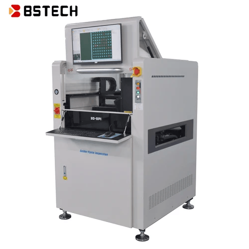
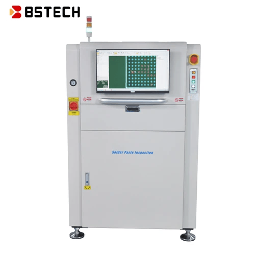
Automated Optical Inspection is a sophisticated technique that utilizes high-resolution cameras and specialized software to detect defects in PCBs during the manufacturing process. Unlike traditional methods, which often rely on manual checks, optical inspection provides real-time feedback and analysis of circuit boards. This precision automated approach not only speeds up the inspection process but also allows for greater consistency in identifying flaws that could compromise product performance.
Importance of Precision in Circuit Board Manufacturing
Precision is critical in circuit board manufacturing as even the slightest error can lead to catastrophic failures in electronic devices. With consumers demanding higher quality and reliability from their gadgets, manufacturers must prioritize accuracy throughout the PCB manufacturing process. Implementing automated inspection systems ensures that every aspect of circuit board production adheres to exact specifications, minimizing risks and enhancing overall product quality.
How Automated Inspection Enhances PCB Quality
Automated inspection plays a pivotal role in enhancing PCB quality by systematically eliminating human error from the equation. By employing advanced algorithms to analyze images captured during production, this technology can detect inconsistencies that might go unnoticed by human inspectors. Consequently, manufacturers benefit from improved reliability and fewer recalls or repairs—ultimately leading to greater customer satisfaction and trust in their products.
What is Automated Optical Inspection

Automated Optical Inspection (AOI) is a pivotal technology in the realm of circuit board manufacturing, designed to ensure precision and quality throughout the production process. This technique utilizes advanced imaging systems to scrutinize PCB boards for defects, ensuring that each component is correctly placed and functioning as intended. By leveraging automated inspection, manufacturers can achieve higher levels of accuracy and consistency compared to traditional methods.
Definition and Technology Behind Optical Inspection
Optical inspection refers to the use of cameras and sophisticated software algorithms to analyze images of circuit boards during the manufacturing process. These systems capture high-resolution images of PCBs and compare them against predefined standards, identifying any discrepancies or defects with remarkable speed and accuracy. The technology behind optical inspection includes 2D and 3D imaging techniques that allow for detailed analysis of surface mount devices, solder joints, and overall board integrity.
Key Applications in PCB Manufacturing
In PCB manufacturing, automated optical inspection plays a crucial role at various stages, including pre-assembly verification, post-reflow inspection, and final product quality checks. By implementing AOI systems early in the production cycle, manufacturers can detect misalignments or missing components before they lead to costly errors down the line. Additionally, optical inspection is invaluable for ensuring compliance with industry standards in sectors like consumer electronics and automotive applications.
Comparing Manual vs. Automated Inspection
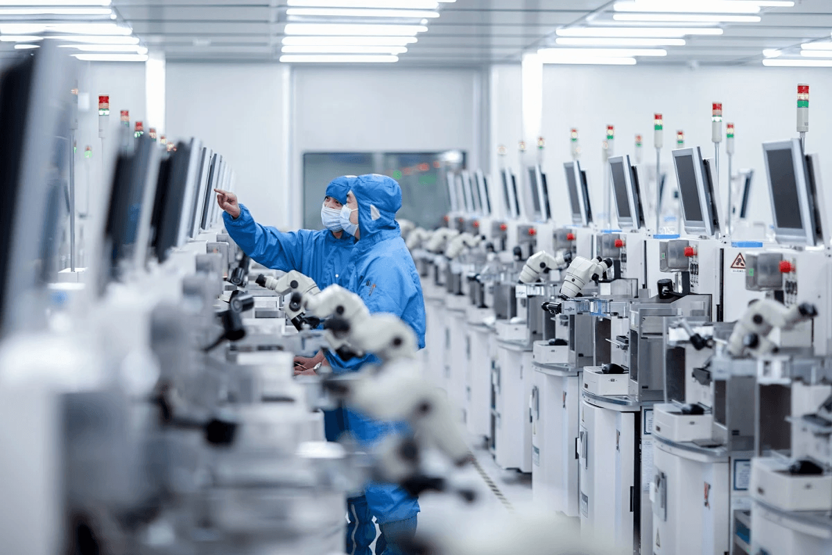
When it comes to inspecting circuit boards, manual methods have long been the norm; however, they are fraught with limitations such as human error and inconsistencies in judgment. In contrast, automated inspection offers precision that far surpasses what human inspectors can achieve alone—a significant advantage when scaling up production volumes in PCB manufacturing. With automatic inspection systems handling repetitive tasks efficiently, manufacturers can focus their resources on innovation while maintaining high-quality standards across all products.
Benefits of Optical Inspection in PCB Manufacturing

In the fast-paced world of circuit board manufacturing, precision is king. Automated optical inspection (AOI) technology has emerged as a game-changer, offering numerous benefits that streamline production processes and enhance quality assurance. By integrating optical inspection into PCB manufacturing, companies can experience significant improvements in efficiency and reliability.
Increasing Efficiency and Reducing Production Time
One of the primary advantages of optical inspection is its ability to increase efficiency in PCB board manufacturing. With automated inspection systems, manufacturers can rapidly scan circuit boards for defects without the delays associated with manual inspections. This not only speeds up production time but also allows for a more streamlined workflow, enabling teams to focus on other critical aspects of circuit board production.
Furthermore, precision automated systems can detect issues that might elude human inspectors, ensuring that only high-quality products move forward in the production line. By minimizing bottlenecks and enhancing throughput, companies can meet growing demands while maintaining high standards of quality. Ultimately, investing in automatic inspection technologies translates to shorter lead times and greater customer satisfaction.
Enhancing Quality Control and Reliability
Quality control is paramount in PCB manufacturing, where even minor defects can lead to catastrophic failures in electronic devices. Optical inspection acts as a powerful ally in this arena by providing real-time feedback on the integrity of each circuit board produced. With advanced imaging capabilities, automated inspection systems identify inconsistencies such as misalignments or soldering errors with remarkable accuracy.
Moreover, these systems offer comprehensive data analytics that help manufacturers track performance over time and identify recurring issues before they escalate into larger problems. The result? Enhanced reliability across the entire product line and a reduction in costly recalls or repairs due to defective boards. In an industry where reputation hinges on quality assurance, embracing optical inspection is not just beneficial; it's essential.
Minimizing Human Error in Circuit Board Production
Human error remains one of the most significant challenges faced by manufacturers during circuit board production processes. Even the most skilled inspectors are susceptible to fatigue or oversight when manually checking boards for defects; this is where automated optical inspection shines brightest. By replacing subjective manual checks with objective machine evaluations, companies can drastically reduce error rates associated with human judgment.
Automated systems provide consistent results regardless of external conditions such as lighting or inspector fatigue—factors that often compromise manual inspections' effectiveness. As a result, manufacturers achieve higher levels of accuracy throughout their PCB manufacturing processes while fostering an environment where workers can concentrate on more complex tasks requiring creativity and problem-solving skills rather than repetitive inspections.
In conclusion, incorporating optical inspection into PCB manufacturing offers compelling advantages ranging from increased efficiency to enhanced quality control and reduced human error risks—all vital components for thriving in today's competitive electronics landscape.
Case Study: Bensun Technology Co., Ltd.

Bensun Technology Co., Ltd. stands out as a pioneer in the realm of automated inspection solutions, particularly for the circuit board manufacturing industry. Their innovative optical inspection systems are designed to enhance precision and efficiency in PCB board manufacturing. By leveraging state-of-the-art technology, Bensun has managed to streamline production processes while ensuring top-notch quality control.
Overview of Bensun’s Inspection Solutions
Bensun offers a comprehensive suite of optical inspection solutions tailored specifically for PCB manufacturing. Their systems utilize advanced imaging technologies that enable precise automated detection of defects on circuit boards, significantly improving the accuracy of quality assurance processes. With features like real-time data analysis and adaptive learning algorithms, Bensun’s automatic inspection solutions not only enhance performance but also adapt to evolving manufacturing needs.
Impact of Automated Inspection on Production Lines
The integration of automated inspection within Bensun's production lines has resulted in remarkable improvements in efficiency and throughput. By replacing traditional manual checks with precision automated systems, they have drastically reduced production time while maintaining high standards for quality control in circuit board manufacturing. This shift has allowed Bensun to increase their output without compromising on reliability, showcasing how effective automated inspection can be in modern PCB board manufacturing environments.
Success Stories in Consumer Electronics and Automotive
Bensun's success stories are abundant, particularly within consumer electronics and automotive sectors where precision is paramount. For instance, by implementing their optical inspection technology, a leading consumer electronics manufacturer reported a 30% reduction in defect rates across their product lines—an impressive feat that underscores the value of automation in quality assurance. Similarly, an automotive client benefited from enhanced reliability through improved defect detection during the assembly process, illustrating how critical optical inspection is for safety-critical applications.
Innovations in Automated Inspection Technology
The landscape of automated inspection technology is evolving rapidly, driven by the relentless pursuit of precision in circuit board manufacturing. As manufacturers seek to enhance quality control and efficiency, innovations in optical inspection are leading the charge. These advancements not only improve the accuracy of inspections but also pave the way for smarter production processes.
Emerging Technologies in Optical Inspection
Emerging technologies in optical inspection are transforming how PCB manufacturing operates. Advanced algorithms and artificial intelligence (AI) are now integrated into automated inspection systems, allowing for real-time analysis and decision-making during the production process. This shift towards precision automated inspection means that defects can be identified earlier, reducing waste and ensuring higher quality circuit boards.
Additionally, 3D imaging technologies are gaining traction within the realm of optical inspection, providing a more comprehensive view of PCB assemblies than traditional 2D methods. By utilizing multiple angles and depths, these systems enhance defect detection capabilities significantly. As a result, manufacturers can achieve unprecedented levels of accuracy in their automatic inspection processes.
Integration with Industry 4.0 and Smart Factories
The integration of automated optical inspection with Industry 4.0 principles is revolutionizing circuit board manufacturing practices worldwide. Smart factories leverage interconnected devices and data analytics to optimize production lines; incorporating advanced optical inspection systems into this framework allows for seamless monitoring and adjustment during manufacturing runs. This synergy enhances operational efficiency while ensuring that each PCB meets stringent quality standards.
Moreover, real-time data from automated inspections can be analyzed to predict potential failures or bottlenecks before they occur, enabling proactive maintenance strategies that further streamline operations. The combination of smart technology with precision automated solutions creates an environment where human oversight is minimized while quality assurance remains paramount in PCB board manufacturing.
Future Trends in Automated Inspection for PCBs
Looking ahead, several trends will shape the future of automated optical inspection within PCB manufacturing environments. One significant trend is the increasing use of machine learning algorithms to improve defect recognition capabilities continuously; as these systems learn from past inspections, they become increasingly adept at identifying subtle anomalies that may have previously gone unnoticed.
Another promising development is the rise of collaborative robots (cobots) that work alongside human operators to enhance productivity without compromising on quality or safety standards during automatic inspections. These cobots can handle repetitive tasks such as visual checks while allowing skilled workers to focus on more complex aspects of circuit board production.
Finally, as sustainability becomes a focal point across industries, innovations aimed at reducing energy consumption during optical inspections will likely gain momentum—helping manufacturers achieve both environmental goals and cost savings simultaneously in their PCB manufacturing processes.
Challenges and Limitations of Automated Optical Inspection

While automated optical inspection (AOI) has revolutionized circuit board manufacturing, it is not without its challenges. The transition from manual to precision automated systems can be fraught with obstacles, including the initial costs of equipment and the need for skilled personnel to operate these advanced machines. Additionally, integrating AOI into existing production lines may require significant adjustments in workflow and processes, which can lead to temporary disruptions.
Common Obstacles in Implementation
One of the primary hurdles in implementing automated inspection systems is the high upfront investment required for state-of-the-art optical inspection technology. Many manufacturers are hesitant to allocate substantial resources without a clear understanding of return on investment (ROI). Furthermore, training staff to effectively use these sophisticated systems can be time-consuming and may temporarily reduce productivity during the learning curve.
Another challenge lies in the compatibility of new AOI systems with existing machinery within circuit board manufacturing environments. Manufacturers often face difficulties when trying to integrate automatic inspection solutions into legacy production lines that were not designed with automation in mind. This lack of compatibility can lead to inefficiencies and increased downtime as teams work through technical issues.
Addressing Limitations of Current Technologies
Despite their many advantages, current optical inspection technologies do have limitations that need addressing for broader adoption in PCB manufacturing. For instance, while AOI excels at detecting surface defects such as misalignment or soldering issues, it may struggle with more complex problems like internal defects or material inconsistencies within multilayer circuit boards. To enhance reliability further, ongoing research is essential to improve detection capabilities across various defect types.
Moreover, environmental factors such as lighting conditions and surface reflections can significantly impact the accuracy of automated inspections. Manufacturers must ensure that their facilities maintain optimal conditions for effective operation; otherwise, they risk compromising quality assurance efforts during PCB board manufacturing processes. As technology evolves, developing adaptive algorithms that account for these variables will be crucial in overcoming current limitations.
Balancing Cost and Quality in PCB Manufacturing
Finding a balance between cost-efficiency and quality assurance remains a critical concern for companies venturing into automated optical inspection solutions. While investing in precision automated systems can yield significant long-term savings through reduced errors and improved throughput rates, the initial costs might deter smaller manufacturers from making this leap forward. Therefore, businesses must carefully assess their specific needs and potential ROI before committing resources.
Additionally, maintaining high-quality standards while managing operational expenses requires continuous evaluation of both processes and technologies used in PCB manufacturing. Companies should consider adopting a phased approach when integrating automatic inspection technologies—starting small before scaling up—to minimize financial risks while still reaping the benefits of enhanced quality control measures over time. Ultimately, striking this balance will empower manufacturers to achieve excellence without sacrificing profitability.
Conclusion
The journey of automated inspection in electronics is just beginning, and the future looks incredibly promising. With advancements in technology, precision automated systems are set to redefine circuit board manufacturing processes. As industries continue to embrace these innovations, the role of automated inspection will become even more integral to ensuring quality and efficiency.
The Future of Automated Inspection in Electronics
Automated inspection technologies are evolving rapidly, incorporating artificial intelligence and machine learning to enhance their capabilities. This evolution will enable even more precise optical inspection methods that can adapt and learn from past errors, leading to fewer defects in PCB board manufacturing. As manufacturers strive for greater efficiency and lower costs, the demand for sophisticated automated inspection solutions will only increase.
Why Optical Inspection is Essential for Quality Assurance
Optical inspection serves as a critical component in maintaining high standards of quality assurance within the PCB manufacturing landscape. By leveraging advanced imaging techniques, this method not only identifies defects but also provides insights into potential improvements in circuit board production processes. Ultimately, implementing optical inspection ensures that products meet rigorous industry standards while minimizing costly rework or recalls.
Transforming PCB Manufacturing with Precision Technology
The integration of precision technology into PCB manufacturing has revolutionized how circuit boards are produced and inspected. Automated optical inspection systems allow manufacturers to achieve unparalleled accuracy while significantly reducing production time and human error risks. As these technologies continue to advance, they promise a future where every circuit board produced is a testament to excellence in quality and reliability.
