Introduction

In the fast-paced world of electronics, where precision is paramount, Automated Optical Inspection (AOI) has emerged as a game-changer in the realm of SMT manufacturing. This technology provides a crucial layer of quality assurance in printed circuit assembly (PCA), ensuring that every solder joint and component placement meets stringent specifications. As we delve into the intricacies of AOI inspection, it becomes clear that its role extends far beyond mere detection; it is integral to maintaining the integrity of circuit card assembly processes.
Understanding Automated Optical Inspection
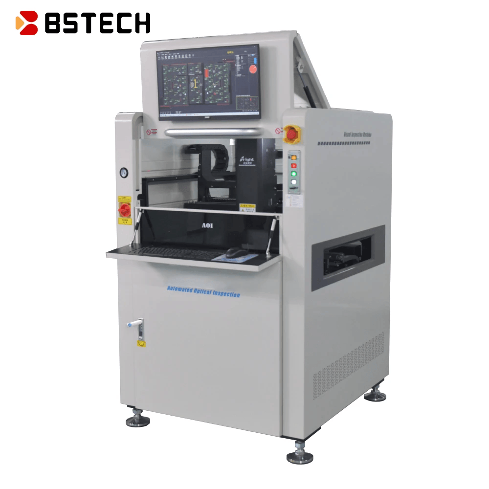
Automated Optical Inspection (AOI) refers to advanced imaging technologies used to evaluate the quality of PCB assembly manufacturing by examining solder paste application and component placement. By employing high-resolution cameras and sophisticated algorithms, AOI systems can identify defects that may lead to costly failures in electronic devices. This non-contact inspection technique significantly enhances both speed and accuracy compared to traditional manual methods, making it a vital tool for manufacturers striving for excellence in their PCB assembly board production.
The Importance of Solder Paste Inspection
Solder paste inspection plays a pivotal role in ensuring optimal performance within electronic assemblies. Proper application of solder paste is essential for creating reliable electrical connections on PCBs; any inconsistencies can lead to defects such as bridging or insufficient solder joints. By integrating AOI inspection into the solder paste phase of PCB manufacturing assembly, companies can dramatically reduce defects and waste while improving overall product reliability.
Key Technologies Behind Inspection Systems
The effectiveness of AOI systems hinges on several key technologies that drive their performance in detecting anomalies during production processes. High-resolution cameras capture detailed images of PCBs at various angles, while machine learning algorithms analyze these images against predefined criteria for quick defect identification. Additionally, advancements in lighting techniques enhance visibility and contrast during optical inspection, allowing for more accurate assessments—critical elements that underscore why investing in robust AOI solutions is essential for modern electronics manufacturers.
The Role of AOI in SMT Manufacturing

Automated Optical Inspection (AOI) plays a pivotal role in the realm of Surface Mount Technology (SMT) manufacturing, particularly in the context of printed circuit assembly (PCA). By integrating advanced imaging technology, AOI systems can detect defects that may go unnoticed during manual inspection processes. This enhancement not only improves the quality of each circuit card assembly but also streamlines production workflows, ensuring that every PCB assembly board meets rigorous standards.
How AOI Inspection Enhances Quality
The implementation of AOI inspection in SMT processes significantly enhances quality control by identifying defects early in the production cycle. Through high-resolution imaging and sophisticated algorithms, these systems can pinpoint issues such as misaligned components or insufficient solder paste application on PCB manufacturing assembly lines. By catching these problems before they escalate, manufacturers can reduce rework costs and ensure that their products maintain high reliability and performance.
Moreover, AOI inspection facilitates consistent monitoring throughout the production process. This continuous oversight helps establish benchmarks for quality assurance, ultimately leading to improved outcomes in circuit card assembly. The result is a more robust final product that meets customer expectations while minimizing waste associated with defective units.
Integration with Production Lines
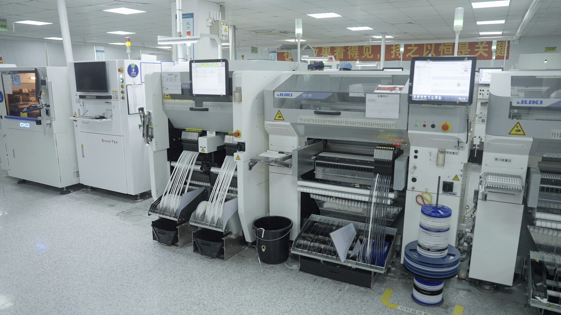
Integrating AOI inspection into existing production lines is not just a technical upgrade; it’s a strategic move towards enhanced efficiency and quality assurance in PCB assembly manufacturing. Modern AOI systems are designed to seamlessly fit into various stages of the SMT process, from solder paste inspection to final product evaluation. This adaptability means manufacturers can implement optical inspection without disrupting their established workflows.
Furthermore, real-time data generated by these systems provides valuable insights into production performance and potential bottlenecks. With this information at their fingertips, operators can make informed decisions about adjustments needed on-the-fly to optimize output and maintain quality standards across all PCB assembly boards produced. Ultimately, this integration fosters a culture of continuous improvement within manufacturing environments.
Case Studies of Successful Implementation
Several industry leaders have successfully implemented AOI inspection systems to revolutionize their SMT manufacturing processes, showcasing tangible benefits across various applications. For example, one prominent electronics manufacturer reported a 30% reduction in defect rates after incorporating automated optical inspection into their printed circuit assembly workflow. This significant decrease not only improved product reliability but also bolstered customer satisfaction ratings.
Another case study highlights how an automotive component supplier utilized solder paste inspection through AOI technology to enhance their quality control measures dramatically. By detecting inconsistencies early on during PCB manufacturing assembly stages, they managed to cut down on costly recalls and warranty claims associated with defective products—saving both time and resources while maintaining their reputation for excellence.
These examples illustrate that adopting advanced technologies like AOI is not merely about keeping up with industry trends; it’s about setting new standards for efficiency and quality within the competitive landscape of electronics manufacturing.
Benefits of Automated Solder Paste Inspection

In the fast-paced world of PCB manufacturing assembly, automated solder paste inspection (SPI) has emerged as a game-changer. By employing advanced optical inspection techniques, manufacturers can significantly enhance the quality of their printed circuit assembly (PCA) processes. This section delves into the benefits of automated solder paste inspection, highlighting its ability to reduce defects and waste, boost production efficiency, and showcase real-world applications in electronics.
Reducing Defects and Waste
One of the most compelling advantages of automated solder paste inspection is its ability to drastically reduce defects in circuit card assembly. Traditional methods often rely on manual checks that can be prone to human error; however, aoi inspection smt systems utilize high-resolution cameras and sophisticated algorithms to detect inconsistencies in solder paste application with remarkable precision. This not only minimizes waste but also ensures that every component on the PCB assembly board is properly aligned and adequately soldered.
Moreover, by identifying issues early in the manufacturing process, companies can implement corrective actions before they escalate into larger problems that could jeopardize entire production runs. This proactive approach not only saves materials but also reduces costly rework and scrap rates associated with defective boards. Ultimately, embracing automated solder paste inspection leads to a more efficient use of resources while maintaining high-quality standards.
Increasing Production Efficiency
Automated solder paste inspection contributes significantly to increasing production efficiency within PCB assembly manufacturing lines. By integrating aoi inspection smt systems directly into production workflows, manufacturers can achieve faster turnaround times without compromising on quality control measures. These systems operate at high speeds while providing real-time feedback on the state of each printed circuit assembly process.
Additionally, consistent monitoring through optical inspection allows for streamlined operations; any deviations from standard practices can be swiftly addressed without halting production entirely. The result is an agile manufacturing environment where productivity flourishes alongside quality assurance practices—ultimately leading to higher output rates and improved profitability for businesses involved in PCB manufacturing assembly.
Real-World Applications in Electronics
The benefits of automated solder paste inspection extend beyond theoretical advantages; numerous real-world applications demonstrate its effectiveness across various sectors within electronics manufacturing. For instance, leading companies specializing in consumer electronics have successfully integrated SPI technology into their production lines to ensure flawless performance in complex devices like smartphones and tablets—where even minor defects can lead to significant failures.
Moreover, industries such as automotive electronics are increasingly adopting automated optical inspection techniques for their critical components like control units and sensors that demand impeccable reliability under challenging conditions. As these sectors continue evolving toward more intricate designs with tighter tolerances, utilizing advanced solder paste inspections will become indispensable for maintaining product integrity throughout the entire lifecycle—from initial design through final assembly.
Bensun Technology's AOI Solutions

Bensun Technology has established itself as a leader in the field of automated optical inspection (AOI) systems tailored for the SMT industry. Their innovative solutions focus on enhancing quality control in printed circuit assembly (PCA) and circuit card assembly (CCA), ensuring that every solder paste inspection is thorough and reliable. With cutting-edge technology, Bensun aims to streamline PCB manufacturing assembly processes while minimizing defects and waste.
Overview of Bensun Offerings
Bensun offers a comprehensive range of AOI inspection SMT solutions designed to meet the diverse needs of electronics manufacturers. Their systems are equipped with advanced optical inspection capabilities that ensure accurate detection of defects during solder paste inspection and PCB assembly manufacturing. From entry-level models to high-end machines, Bensun’s offerings cater to various production scales and complexities, making them an ideal choice for any PCB assembly board requirement.
Specialized Equipment for Diverse Industries
In addition to standard AOI systems, Bensun provides specialized equipment tailored for various industries including automotive, telecommunications, and consumer electronics. This versatility allows manufacturers in different sectors to achieve optimal results in their printed circuit assembly processes while maintaining rigorous quality standards through effective solder paste inspection techniques. By focusing on industry-specific needs, Bensun ensures that their optical inspection systems deliver maximum efficiency across all applications.
Customer Testimonials and Success Stories
Customers rave about the transformative impact of Bensun's AOI solutions on their production lines. Many have reported significant reductions in defects during PCB manufacturing assembly, leading to enhanced product reliability and customer satisfaction. Success stories highlight how companies leveraging Bensun’s technology have not only improved their quality control measures but also increased overall productivity within their circuit card assembly operations.
Choosing the Right Inspection System
Selecting the appropriate inspection system for your printed circuit assembly (PCA) is crucial in ensuring quality and efficiency in PCB manufacturing assembly. With various options available, understanding the unique requirements of your production line is essential. This section will explore key factors to consider when choosing an AOI inspection SMT system, its scalability and adaptability, and how to compare leading brands and technologies effectively.
Factors to Consider for AOI Inspection SMT
When evaluating AOI inspection SMT systems, several factors come into play that can significantly influence your decision. First, consider the specific requirements of your circuit card assembly processes; different systems may excel in inspecting various components or solder paste applications. Additionally, think about the speed of inspection—faster systems can enhance throughput but must maintain accuracy to prevent defects in PCB assembly manufacturing.
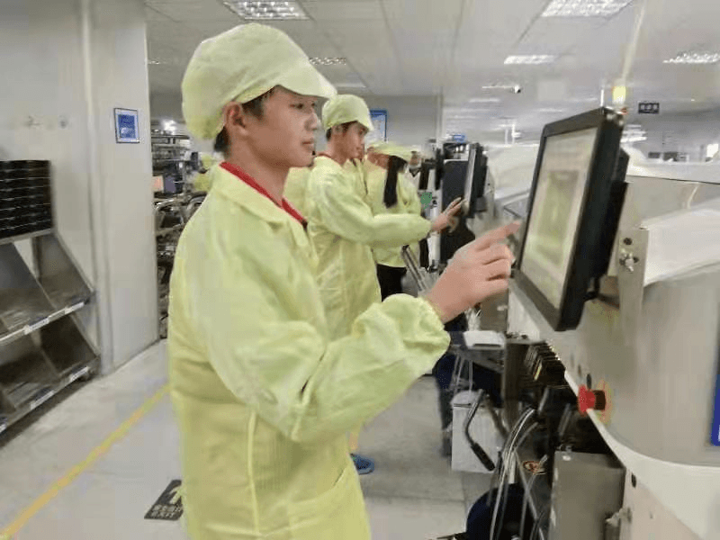
Another critical aspect is the ease of integration with existing production lines. An AOI system should seamlessly connect with other machinery involved in solder paste inspection and overall PCB manufacturing assembly processes to ensure a smooth workflow. Lastly, user-friendliness plays a significant role; operators should be able to navigate software and hardware without extensive training or technical expertise.
Scalability and Adaptability of Equipment
Scalability is vital when choosing an optical inspection system as it determines how well the equipment can grow alongside your business needs. As demand fluctuates or product lines change, having a flexible AOI solution allows manufacturers to adapt without overhauling their entire setup. Look for systems that support upgrades or modular components so you can easily enhance capabilities without hefty investments.
Adaptability also extends to software updates; an effective AOI inspection SMT system should regularly receive improvements that keep pace with technological advancements in printed circuit assembly techniques. Moreover, consider whether the equipment can handle varying sizes of PCB assembly boards or different types of solder paste applications efficiently—this versatility ensures longevity and relevance as industry standards evolve.
Comparing Leading Brands and Technologies
With numerous companies offering AOI solutions, it's essential to conduct thorough research when comparing leading brands and technologies available on the market today. Start by reviewing customer testimonials and case studies that showcase real-world performance; this information provides valuable insights into reliability and effectiveness during actual PCB manufacturing assembly scenarios.
Next, assess each brand's technological innovations—some may incorporate advanced features like artificial intelligence or machine learning capabilities that enhance defect detection rates during solder paste inspections significantly. Finally, don't forget about customer support; reliable service can make all the difference when troubleshooting issues with your optical inspection equipment.
Future Trends in Optical Inspection

The landscape of optical inspection is evolving rapidly, driven by technological advancements and the ever-increasing demand for precision in printed circuit assembly (PCA). As manufacturers strive to enhance quality control, innovations in inspection technologies are paving the way for more efficient and accurate processes. The integration of cutting-edge tools not only improves solder paste inspection but also streamlines the entire PCB manufacturing assembly workflow.
Innovation in Inspection Technologies
Recent innovations have transformed aoi inspection smt into a powerhouse of efficiency and accuracy. Advanced imaging techniques, such as 3D profiling and multispectral analysis, allow for better detection of defects in circuit card assembly. These technologies enable inspectors to identify issues that traditional methods might overlook, ensuring that every PCB assembly board meets rigorous quality standards.
Moreover, automation is becoming integral to inspection processes; machines equipped with sophisticated algorithms can analyze vast amounts of data at lightning speed. This shift not only reduces human error but also enhances the overall reliability of solder paste inspection results. As these innovations continue to emerge, we can expect a significant reduction in production costs and an increase in output quality across the industry.
The Rise of AI and Machine Learning
Artificial intelligence (AI) and machine learning are set to revolutionize aoi inspection smt by introducing smart algorithms that learn from previous inspections. These systems can adapt over time, improving their ability to detect anomalies during printed circuit assembly processes. By analyzing patterns from past inspections, AI-driven solutions can predict potential failures before they occur, allowing manufacturers to address issues proactively.
Furthermore, machine learning enhances data analysis capabilities by enabling real-time feedback loops within production lines. This means that as defects are detected during solder paste inspection, adjustments can be made instantly to prevent future occurrences—a game-changer for PCB manufacturing assembly efficiency. The combination of AI with optical inspection technologies will lead to smarter factories where human oversight is complemented by intelligent systems.
Predictions for the SMT Industry
Looking ahead, we anticipate several key trends shaping the future of optical inspection in the SMT industry. First off, increased collaboration between hardware manufacturers and software developers will yield more integrated solutions tailored specifically for circuit card assembly needs. This synergy will likely result in multifunctional equipment capable of handling various aspects of PCB assembly manufacturing seamlessly.
Additionally, sustainability will become a focal point; companies will prioritize eco-friendly materials and processes while maintaining high-quality standards through effective solder paste inspection techniques. Finally, as industries continue to embrace digital transformation, we expect a surge in remote monitoring capabilities within AOI systems—allowing engineers worldwide to oversee operations without being physically present on-site.
In summary, innovation is driving the future trends within optical inspection technologies for PCB manufacturing assemblies—where efficiency meets precision through advanced methods like AI integration and sustainable practices.
Conclusion

In the rapidly evolving landscape of printed circuit assembly (PCA), the significance of automated optical inspection (AOI) in SMT manufacturing cannot be overstated. As we have explored, AOI inspection not only enhances quality control but also ensures that the final products meet stringent industry standards. By integrating these advanced systems into PCB manufacturing assembly processes, companies can significantly reduce defects and improve overall production efficiency.
Enhancing Quality Control with AOI
Implementing AOI inspection in circuit card assembly drastically improves quality assurance protocols. This technology allows for real-time monitoring of solder paste application and component placement, identifying potential issues before they escalate into costly defects. With precise optical inspection capabilities, manufacturers can ensure that every PCB assembly board adheres to high-quality standards, thus boosting customer confidence and satisfaction.
Maximizing Efficiency through Solder Paste Inspection
Solder paste inspection is a critical step in optimizing PCB assembly manufacturing processes. By detecting discrepancies early on, manufacturers can minimize waste and reduce rework time associated with faulty assemblies. This proactive approach not only streamlines production but also leads to significant cost savings, allowing companies to allocate resources more effectively while maintaining high throughput rates.
The Future of Automated Inspection Systems
Looking ahead, the future of automated inspection systems appears promising as innovation continues to drive advancements in optical inspection technologies. The rise of AI and machine learning will likely enhance AOI capabilities further, enabling systems to learn from past inspections and adapt accordingly for even greater accuracy. As the SMT industry embraces these cutting-edge solutions, we can anticipate a new era of efficiency and reliability in printed circuit assembly.
