Introduction
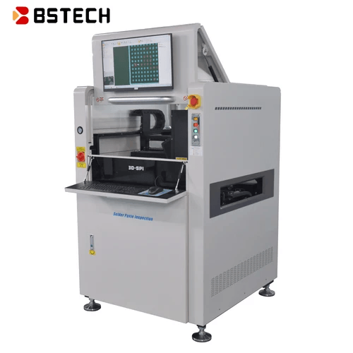
In the fast-paced world of electronics manufacturing, quality control is paramount, and one of the most effective tools at our disposal is the automated optical inspection machine. This technology plays a crucial role in ensuring that printed circuit boards (PCBs) meet stringent quality standards before they are assembled into final products. As we delve deeper into this topic, we'll explore what an automated optical inspection machine is, how it differs from other inspection methods like ICT, and the essential functions it performs in PCB assembly.
Understanding Automated Optical Inspection
Automated Optical Inspection (AOI) refers to a non-contact inspection method that uses cameras and advanced software to detect defects on PCBs. What is an automated optical inspection? Essentially, it's a sophisticated system designed to identify issues such as misaligned components, soldering defects, or any other irregularities that could compromise product performance. By employing AOI systems, manufacturers can significantly enhance their quality control processes and maintain high production standards.
The Role of AOI in PCB Assembly
In PCB assembly, AOI serves as a critical checkpoint that helps catch potential problems early in the manufacturing process. What does an AOI do? It scans each board with precision and provides instant feedback on its integrity—allowing for quick corrective actions if necessary. The implementation of automated optical inspection PCB not only improves product reliability but also streamlines workflows by reducing manual inspections.
Key Benefits of AOI Systems
The advantages of adopting an AOI system are manifold; they include increased accuracy in defect detection and faster inspection times compared to traditional methods. By understanding what is the difference between AOI and ICT, manufacturers can make informed decisions about which technology best suits their needs for specific applications. Additionally, with advancements like 3D AOI for PCB assembly becoming more prevalent, companies can leverage even greater levels of detail in their inspections—ensuring top-notch quality across all products.
What is an Automated Optical Inspection?
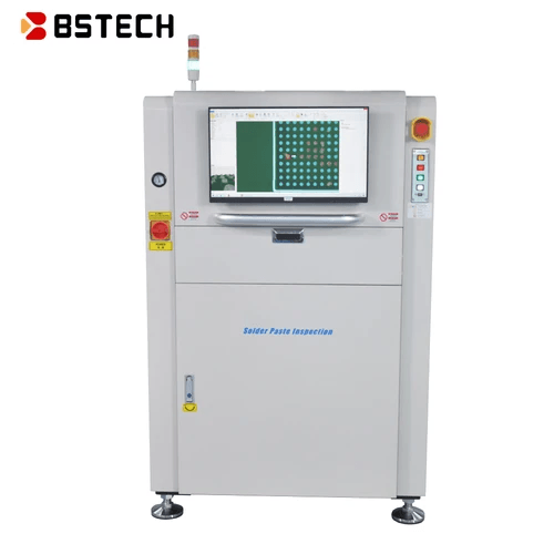
Automated Optical Inspection (AOI) is a crucial technology in the realm of electronics manufacturing, particularly for PCB assembly. This sophisticated process utilizes advanced imaging techniques to detect defects on printed circuit boards (PCBs) before they proceed to the next stages of production. By employing an automated optical inspection machine, manufacturers can ensure that their products meet stringent quality standards while minimizing human error.
Definition and Purpose of AOI
So, what is an automated optical inspection? Simply put, AOI refers to a method that uses cameras and software algorithms to analyze the surface of PCBs for any irregularities or defects. The primary purpose of AOI is to enhance the reliability and performance of electronic devices by identifying issues such as misaligned components, soldering defects, or even missing parts before they lead to larger problems down the line.
The implementation of automated optical inspection PCB systems significantly reduces the likelihood of faulty products reaching consumers. In essence, AOI acts as a vigilant guardian in manufacturing processes, ensuring that only high-quality boards make it into finished products. This proactive approach not only boosts customer satisfaction but also safeguards manufacturers from costly recalls and reputational damage.
How AOI Enhances Quality Control
The role of AOI in enhancing quality control cannot be overstated; it serves as a critical checkpoint within the production line. By integrating an automated optical inspection machine into their processes, manufacturers can achieve higher levels of precision and consistency in defect detection compared to traditional methods. This enhanced level of scrutiny enables quicker identification and rectification of issues before they escalate.
Moreover, incorporating AOI helps streamline production workflows by reducing dependency on manual inspections which are often time-consuming and prone to human error. With its ability to process thousands of images per minute while maintaining accuracy, AOI supports manufacturers in achieving tighter tolerances and better overall product quality. As a result, businesses can expect reduced scrap rates and improved yield percentages—essential metrics for any efficient operation.
The Technology Behind Automated Optical Inspection Machines
At the heart of every automated optical inspection machine lies sophisticated technology designed for high-speed image capture and analysis. These machines typically employ high-resolution cameras combined with powerful lighting systems that illuminate PCBs at various angles to reveal hidden defects effectively. Advanced software algorithms then analyze these images against predefined criteria or reference models.
The technology behind 3D AOI for PCB assembly takes this concept further by adding depth perception capabilities that allow for more comprehensive inspections than traditional 2D systems can provide alone. With 3D imaging technology, inspectors can identify issues related not just to surface appearance but also component height variations or solder fillet profiles—areas where conventional methods might fall short. Such advancements highlight how far we’ve come from basic visual inspections toward embracing cutting-edge solutions in manufacturing quality assurance.
What is the Difference Between AOI and ICT?
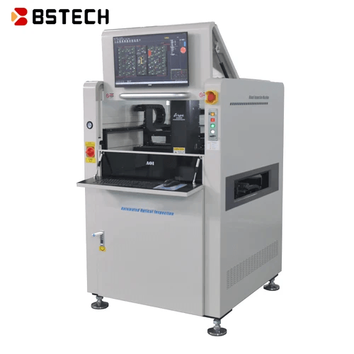
In the realm of PCB manufacturing, understanding the differences between Automated Optical Inspection (AOI) and In-Circuit Testing (ICT) is crucial. Both methods aim to ensure product quality, but they employ distinct techniques and serve different purposes. This section delves into these inspection methods, highlighting their unique features and applications in the industry.
Comparing Inspection Methods
Automated Optical Inspection machines utilize high-resolution cameras to capture images of PCBs and compare them against pre-defined templates, identifying defects such as missing components or misalignments. On the other hand, ICT involves electrical testing of assembled boards to verify that each component functions correctly within a circuit. While AOI excels at visual inspections, ICT is more focused on functional testing, making it an essential complement rather than a direct competitor.
The choice between AOI and ICT often depends on specific project requirements; for example, AOI can quickly assess large volumes of PCBs during initial production stages, while ICT is typically employed later in the assembly process to ensure electrical integrity. Additionally, AOI provides immediate feedback for rapid adjustments in manufacturing processes, whereas ICT may require more time due to its detailed testing protocols. Understanding what an automated optical inspection machine can do versus what ICT offers helps manufacturers select the right tool for their quality control arsenal.
Strengths of AOI in PCB Manufacturing
The strengths of Automated Optical Inspection in PCB manufacturing are numerous and impactful. First off, AOI systems can detect a wide range of defects early in the production cycle—whether it’s soldering issues or component placement errors—saving time and resources by addressing problems before they escalate. Furthermore, with advancements like 3D AOI for PCB assembly becoming increasingly prevalent, these systems now provide depth perception capabilities that enhance defect detection beyond traditional 2D imaging.
Another significant advantage of using an automated optical inspection machine lies in its speed; these systems can inspect boards much faster than manual inspections while maintaining high accuracy levels. This efficiency translates into shorter production cycles and reduced labor costs associated with human inspection efforts. Additionally, as manufacturers strive for greater consistency in quality control processes across various production runs, incorporating AOI technology ensures uniformity that manual checks simply cannot match.
When to Choose ICT Over AOI
While Automated Optical Inspection has numerous benefits for PCB assembly processes, there are scenarios where In-Circuit Testing may be preferable or necessary. For instance, if a manufacturer requires thorough verification of component functionality after assembly—particularly when dealing with complex circuits—ICT becomes indispensable due to its ability to test each connection electrically under load conditions that mirror real-world usage scenarios.
Moreover, certain products may demand compliance with stringent industry standards that dictate specific testing protocols; here again lies a strong case for utilizing ICT alongside or instead of AOI systems. It’s also worth noting that some manufacturers might find it beneficial to use both methodologies together: employing an automated optical inspection machine during initial inspections followed by ICT for final validation ensures comprehensive coverage throughout the manufacturing process.
Ultimately, knowing what does an AOI do compared to what does an AOI operator do can help clarify when one method should take precedence over another based on operational goals and product requirements.
What Does an AOI Do?
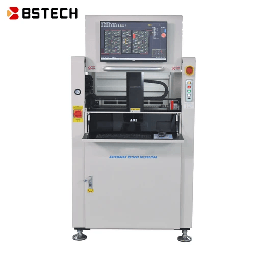
Automated Optical Inspection (AOI) is a game-changer in the world of PCB manufacturing, capable of identifying defects that could derail production quality. But what does an AOI do exactly? It employs advanced imaging technology to scrutinize printed circuit boards (PCBs) for flaws, ensuring that every component is in its rightful place and functioning correctly.
Identifying Defects on PCBs
An automated optical inspection machine scans PCBs with precision, capturing high-resolution images to identify potential defects such as misalignments, soldering issues, and missing components. The system uses sophisticated algorithms to compare the captured images against predefined standards or templates, making it adept at spotting discrepancies that might go unnoticed by the human eye. This capability not only enhances product quality but also significantly reduces the risk of costly errors during later stages of assembly.
The Steps Involved in AOI
The process begins with loading the PCB onto the automated optical inspection machine's conveyor system, where it is positioned for optimal scanning. Next, high-resolution cameras capture detailed images from various angles; this is particularly important when considering new advancements like 3D AOI for PCB assembly that provide depth perception and a more comprehensive view of each board. Once image data is collected, sophisticated software analyzes it for defects and generates a report indicating any areas requiring attention—streamlining decision-making for operators.
Advantages of Automated Optical Inspection Over Manual Inspection
One major advantage of using an automated optical inspection machine over traditional manual inspection methods is speed; AOI can process multiple boards simultaneously without fatigue or error-prone human oversight. Additionally, while manual inspections may miss subtle flaws due to human limitations or distractions, AOI systems utilize consistent algorithms and imaging techniques that ensure thoroughness every time—making them far more reliable in maintaining quality control standards. Ultimately, implementing automated optical inspection PCB processes leads to higher efficiency and significant cost savings by minimizing rework and enhancing overall production quality.
The Role of AOI Operators
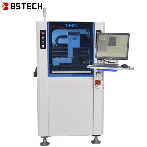
Automated Optical Inspection (AOI) is a crucial component in the PCB assembly process, but it’s the AOI operators who bring this technology to life. These professionals are responsible for ensuring that the automated optical inspection machine functions optimally and delivers accurate results. With their expertise, they help maintain high standards of quality control and efficiency in manufacturing.
Skills Required for AOI Operators
To excel as an AOI operator, a blend of technical and analytical skills is essential. Operators should have a solid understanding of electronics and PCB design principles, which allows them to interpret inspection data effectively. Additionally, problem-solving abilities are crucial when identifying issues that may arise during inspections or with the automated optical inspection machine itself.
Attention to detail is another vital skill; operators must be meticulous in monitoring outputs from the AOI system to ensure no defects go unnoticed. Familiarity with software used for programming and analyzing inspection parameters also enhances an operator's effectiveness. Ultimately, strong communication skills help facilitate collaboration with other team members involved in the PCB assembly process.
Daily Responsibilities of an AOI Operator
What does an AOI operator do on a day-to-day basis? Their responsibilities are diverse and include setting up the automated optical inspection machine for each production run, ensuring it is calibrated correctly to detect any potential defects on PCBs accurately. They also monitor the performance of the system throughout production, making real-time adjustments as necessary.
Daily tasks often involve reviewing inspection data reports generated by the AOI systems to identify trends or recurring issues that may require further investigation. This analysis helps improve overall quality control processes within PCB manufacturing facilities. Additionally, operators frequently collaborate with engineers and technicians to troubleshoot problems or refine inspection protocols based on their findings.
Training and Certification for AOI Professionals
Training is vital for anyone looking to become proficient in operating an automated optical inspection machine effectively. Many companies provide on-the-job training programs tailored specifically for new hires entering positions related to Automated Optical Inspection PCB processes. These programs typically cover both technical skills related to machinery operation as well as quality assurance methodologies.
Certification courses are also available through various professional organizations that focus on electronics manufacturing technologies; these can enhance an operator's credentials significantly in this competitive field. Such certifications not only validate their expertise but also keep them updated about advancements like 3D AOI for PCB assembly technology that continues evolving rapidly.
In summary, skilled AOI operators play a pivotal role in ensuring high-quality standards within PCB assembly operations through their daily responsibilities and ongoing education efforts.
The Rise of 3D AOI for PCB Assembly
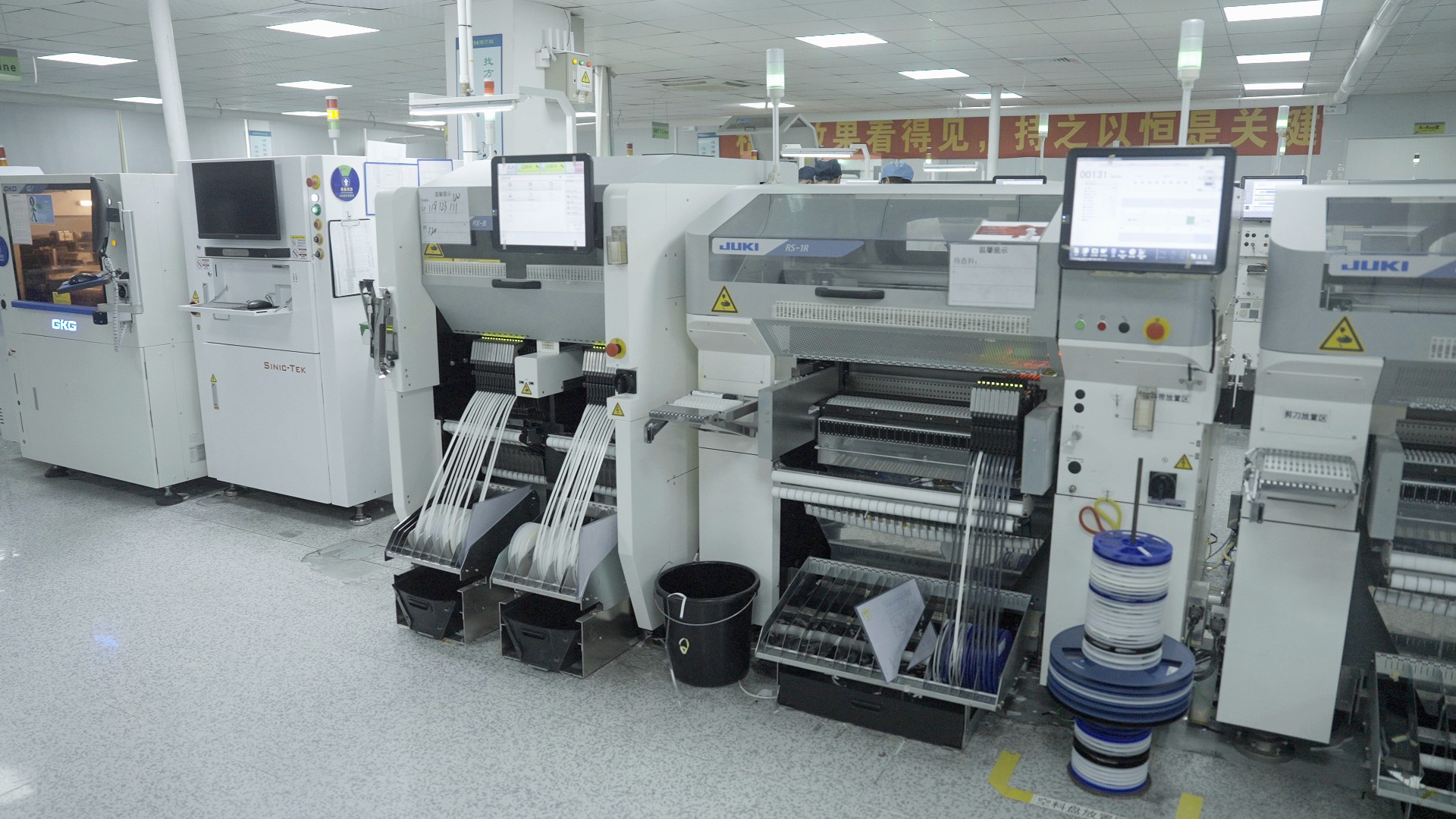
In the world of PCB assembly, the emergence of 3D Automated Optical Inspection (AOI) has revolutionized quality control processes. Traditional 2D inspection methods had their limitations, often missing defects that could compromise performance. With the introduction of 3D inspection technology, manufacturers can now achieve a more thorough analysis, ensuring that every layer and component is scrutinized with precision.
Advantages of 3D Inspection Technology
The advantages of 3D inspection technology in automated optical inspection machines are numerous and compelling. First and foremost, it allows for a comprehensive view of the PCB assembly from multiple angles, making it easier to detect hidden defects that might go unnoticed in a standard 2D scan. Furthermore, this advanced technology enhances depth perception capabilities, enabling operators to differentiate between components more effectively and reduce false positives during inspections.
Another key benefit is improved accuracy in height measurement and component placement validation. This means that what does an AOI do? It not only identifies surface-level defects but also ensures that components are correctly aligned within their designated spaces—an aspect crucial for high-density boards. As manufacturers increasingly adopt this cutting-edge technology, the efficiency gains become evident through reduced rework rates and enhanced product reliability.
Leading 3D AOI Systems in the Market
Several leading systems have emerged as front-runners in the realm of 3D AOI for PCB assembly. Companies like Koh Young Technology and Omron have developed sophisticated automated optical inspection machines equipped with advanced algorithms designed to tackle complex assemblies with ease. Their systems are renowned for their speed and accuracy, providing real-time feedback that helps manufacturers maintain tight quality control throughout production.
Additionally, newer entrants into the market are pushing boundaries with innovative features such as AI-driven defect recognition and user-friendly interfaces that simplify operation for what does an AOI operator do? These advancements make it easier than ever to integrate these systems into existing workflows while maximizing productivity. As competition heats up among these players, we can expect even more groundbreaking developments tailored to meet diverse manufacturing needs.
Future Trends in 3D Automated Optical Inspection
The future trends in 3D automated optical inspection hint at even greater integration of artificial intelligence (AI) and machine learning technologies into AOI systems. These innovations promise to enhance defect detection capabilities further by allowing machines to learn from past inspections—essentially evolving their understanding of what constitutes a defect over time. This evolution will enable manufacturers to achieve unprecedented levels of accuracy while minimizing human error.
Moreover, we can anticipate increased connectivity between automated optical inspection PCB systems and other manufacturing equipment through Industry 4.0 initiatives like IoT integration. Such connectivity will facilitate real-time data sharing across platforms, allowing operators to make informed decisions based on comprehensive analytics rather than isolated metrics alone—what is the difference between AOI and ICT? The answer lies in how interconnected these new technologies will become moving forward.
As we look ahead, it's clear that embracing advancements like 3D AOI will be vital for manufacturers aiming to stay competitive in an ever-evolving landscape focused on quality assurance and efficiency.
Conclusion

In the fast-paced world of PCB manufacturing, the significance of Automated Optical Inspection (AOI) cannot be overstated. This technology has revolutionized quality control processes, ensuring that defects are caught early and efficiently. With its ability to enhance manufacturing efficiency, AOI stands as a cornerstone in modern production lines.
The Impact of AOI on Manufacturing Efficiency
Automated optical inspection machines play a crucial role in streamlining production processes by minimizing human error and increasing throughput. By automating the inspection stages, manufacturers can detect issues like soldering defects or misplaced components more effectively than with traditional methods. This not only leads to higher quality products but also significantly reduces waste and rework costs.
The integration of AOI into PCB assembly lines has shown that what is an automated optical inspection? It’s not just about catching mistakes; it’s about enhancing overall operational efficiency. Companies leveraging automated optical inspection PCB experience faster turnaround times and improved reliability in their products, giving them a competitive edge in the market.
Choosing the Right AOI System for Your Needs
When considering what is the difference between AOI and ICT, it’s essential to evaluate your specific requirements before making a decision on an automated optical inspection machine. Factors such as production volume, types of PCBs being manufactured, and budget constraints all play vital roles in determining which system will best suit your operation.
While both methods have their strengths, understanding what does an AOI do? can help you identify when AOI's capabilities align better with your needs compared to In-Circuit Testing (ICT). Ultimately, selecting the right system involves balancing performance features with cost-effectiveness while ensuring it meets industry standards.
How Bensun Technology Supports AOI Implementation
Bensun Technology stands out as a leader in providing innovative solutions for implementing 3D AOI for PCB assembly systems tailored to various manufacturing environments. Their expertise ensures that companies not only acquire state-of-the-art automated optical inspection machines but also receive comprehensive training on what does an AOI operator do? This support streamlines integration into existing workflows.
With Bensun's commitment to customer satisfaction, businesses can confidently navigate through questions like what is an automated optical inspection? Their guidance helps clients maximize their investment by optimizing operational efficiency while maintaining high-quality standards throughout production cycles.
