Introduction
In the fast-paced world of electronics, ensuring the reliability and quality of printed circuit boards (PCBs) is paramount. Optical inspection plays a crucial role in this process, serving as a vital checkpoint in circuit board production. By implementing advanced techniques like Automated Optical Inspection (AOI), manufacturers can significantly enhance the overall quality of their PCB manufacturing processes.
The Importance of Optical Inspection
Optical inspection is essential for maintaining high standards in PCB board production, as it allows for real-time monitoring and detection of defects that could compromise functionality. With the increasing complexity of electronic devices, effective optical inspection methods have become indispensable for achieving precision in circuit board manufacturing. This proactive approach not only identifies flaws early but also ensures that products meet stringent industry standards.
How AOI Transforms PCB Manufacturing
Automated Optical Inspection revolutionizes printed circuit board production by automating the inspection process, thus reducing human error and increasing throughput. AOI systems utilize sophisticated imaging technology to analyze PCBs at various stages of manufacturing, ensuring that any defects are caught before they escalate into larger issues. This transformation leads to improved efficiency and reliability in circuit board production, allowing manufacturers to keep pace with market demands.
Common Challenges in Circuit Board Production
Despite advancements like AOI, circuit board production still faces several challenges that can hinder efficiency and quality control. Issues such as component misalignment, soldering defects, and contamination can arise during PCB manufacturing processes if not properly monitored through optical inspection techniques. Addressing these challenges with robust optical inspection systems is critical for sustaining high-quality standards in an increasingly competitive industry.
What Is Automated Optical Inspection?

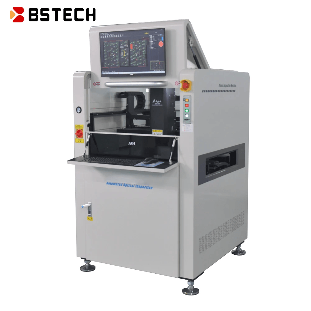
Automated Optical Inspection (AOI) is a critical technology employed in the realm of printed circuit board (PCB) production. It leverages sophisticated imaging systems to detect defects on circuit boards, ensuring that each unit meets stringent quality standards before moving further along the manufacturing line. By integrating AOI into the PCB manufacturing process, companies can significantly enhance their quality control measures and streamline production.
Definition and Overview of AOI
Automated Optical Inspection is a non-contact inspection method that uses cameras and advanced software algorithms to examine circuit boards for defects such as soldering issues, component misalignments, and other anomalies that could affect performance. The process involves capturing high-resolution images of the PCB and comparing them against predefined templates or specifications. This rapid inspection capability allows manufacturers to identify problems early in the circuit board production cycle, reducing waste and increasing overall efficiency.
Role of AOI in PCB Manufacturing
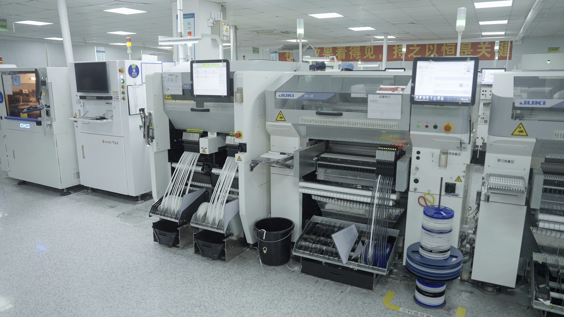
In the world of PCB manufacturing, AOI plays a pivotal role by acting as an early warning system for potential defects. By implementing optical inspection at various stages—such as after soldering or component placement—manufacturers can catch errors before they escalate into costly rework or product failures. This proactive approach not only ensures higher-quality circuit board production but also fosters greater confidence in product reliability among end-users.
Key Technologies Used in AOI
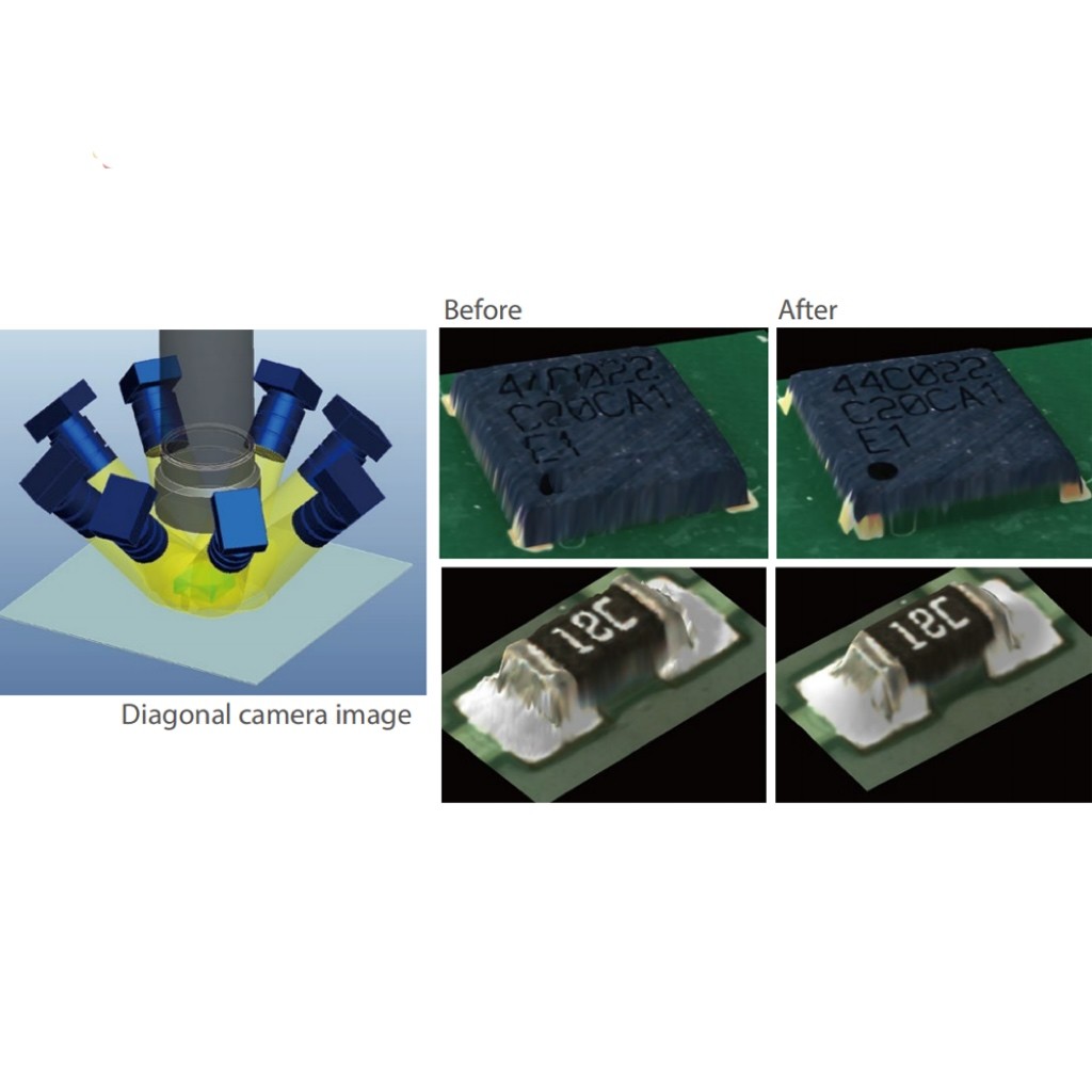
The effectiveness of pcb optical inspection relies on several key technologies that work together seamlessly to deliver accurate results. High-resolution cameras capture detailed images of the PCBs, while specialized lighting techniques enhance visibility by eliminating shadows and reflections that could obscure defects. Additionally, sophisticated software algorithms analyze these images quickly, identifying discrepancies with remarkable precision—making them indispensable tools for modern circuit board manufacturing processes.
Benefits of PCB Optical Inspection

In today’s fast-paced world of electronics, the benefits of PCB optical inspection are manifold and vital for maintaining high standards in circuit board production. As manufacturers strive for quality and efficiency, integrating optical inspection into the printed circuit board production process has become a game changer. From enhancing quality control to reducing costs, the advantages are clear and compelling.
Enhancing Quality Control in PCB Production
Quality control is paramount in PCB manufacturing, where even the smallest defect can lead to significant failures down the line. Automated optical inspection (AOI) systems meticulously examine each circuit board, identifying issues such as misaligned components or soldering defects that might escape human eyes. By implementing effective optical inspection techniques, manufacturers can ensure that only flawless products make it through to assembly, bolstering their reputation for excellence in circuit board production.
Reducing Manufacturing Costs
When it comes to printed circuit board production, cutting costs without sacrificing quality is the Holy Grail for many manufacturers. Optical inspection helps achieve this by catching defects early in the manufacturing process, which reduces waste and minimizes costly rework or recalls later on. By streamlining operations through efficient AOI systems, companies can significantly lower their overall pcb manufacturing expenses while maintaining high-quality standards.
Increasing Production Efficiency
Time is money in circuit board manufacturing; therefore, increasing production efficiency is crucial for staying competitive. Automated optical inspection speeds up the quality control process by rapidly scanning multiple boards simultaneously and providing instant feedback on potential issues. This not only accelerates throughput but also allows teams to focus on optimization strategies rather than constantly troubleshooting errors—ultimately leading to a more agile and productive pcb board production environment.
Key Components of AOI Systems

Automated Optical Inspection (AOI) systems are integral to the realm of PCB manufacturing, ensuring that every circuit board meets rigorous quality standards. To achieve this, several key components work in harmony to deliver precise results. Understanding these components can help manufacturers optimize their circuit board production processes and enhance overall efficiency.
Cameras and Imaging Technology
At the heart of any effective PCB optical inspection system lies advanced cameras and imaging technology. These high-resolution cameras capture detailed images of printed circuit boards, allowing for meticulous examination of each component and solder joint. The ability to discern minute details is crucial in circuit board manufacturing, as even the smallest defect can lead to significant failures down the line.
Modern imaging technologies, such as 2D and 3D imaging systems, further elevate the capabilities of AOI systems. While 2D imaging provides a flat view for quick inspections, 3D imaging offers depth perception that can identify issues like lifted leads or insufficient solder fillets more effectively. This combination ensures that manufacturers can maintain high standards during PCB board production while minimizing errors.
Lighting Techniques for Accurate Inspection
Lighting plays a pivotal role in enhancing the accuracy of optical inspection processes in PCB manufacturing. Various lighting techniques are employed to illuminate circuit boards optimally, revealing defects that might otherwise go unnoticed under standard lighting conditions. Techniques such as bright field, dark field, and polarized light help highlight different aspects of the PCB surface for comprehensive analysis.
Bright field lighting illuminates the entire surface uniformly, making it ideal for detecting color variations or surface defects on printed circuit boards. In contrast, dark field lighting accentuates irregularities by casting shadows on raised features—perfect for spotting solder issues or component misalignments during circuit board production. By employing a mix of these techniques strategically within AOI systems, manufacturers can achieve unparalleled precision in their inspections.
Software Algorithms for Data Analysis
Once images are captured through advanced cameras and illuminated by sophisticated lighting techniques, software algorithms take center stage in processing this data during optical inspection. These algorithms analyze image data to identify defects based on predefined criteria tailored specifically for each type of printed circuit board production process. By automating this analysis, AOI systems significantly reduce human error while increasing throughput.
Moreover, machine learning algorithms are increasingly being integrated into AOI software solutions to enhance defect detection capabilities continually. As these systems learn from previous inspections and adapt over time, they become more proficient at identifying subtle anomalies that may have been previously overlooked during manual inspections in circuit board manufacturing processes. This evolution not only boosts quality assurance but also contributes to overall cost savings by reducing rework rates associated with faulty PCBs.
Applications of Optical Inspection in Electronics

Optical inspection plays a pivotal role across various sectors of electronics, ensuring the reliability and performance of devices we use daily. From consumer gadgets to sophisticated medical equipment, the applications of PCB optical inspection are both diverse and critical. This section delves into specific use cases that highlight the importance of optical inspection in circuit board production.
Use Cases in Consumer Electronics
In the realm of consumer electronics, PCB optical inspection is indispensable for maintaining high-quality standards. Devices like smartphones, tablets, and laptops rely on flawless circuit boards for optimal performance; even minor defects can lead to significant failures. By integrating optical inspection into printed circuit board production, manufacturers can swiftly identify issues such as misaligned components or soldering errors early in the manufacturing process.
Moreover, with the rapid pace of innovation in consumer electronics, manufacturers face increasing pressure to deliver products faster without compromising quality. Automated optical inspection systems not only enhance quality control but also streamline circuit board manufacturing processes by reducing rework and scrap rates. Consequently, this leads to improved customer satisfaction and brand loyalty in a competitive market.
Importance in Automotive and Medical Devices
The automotive industry has undergone a technological transformation with the rise of electric vehicles (EVs) and advanced driver-assistance systems (ADAS). In this context, PCB optical inspection ensures that critical electronic components function reliably under demanding conditions. Any failure within these systems could have dire consequences; hence, rigorous testing through optical inspection is vital during circuit board production.
Similarly, medical devices demand an unparalleled level of precision due to their direct impact on patient safety. The integration of automated optical inspection in medical device manufacturing helps ensure that every printed circuit board meets stringent regulatory standards while minimizing risks associated with faulty components. As such, PCB optical inspection not only safeguards lives but also enhances trust in healthcare technologies.
Role in Semiconductor Manufacturing
Semiconductor manufacturing is another domain where PCB optical inspection proves invaluable due to its complexity and precision requirements. The intricate designs found within semiconductor circuits necessitate meticulous scrutiny during production processes to prevent defects that could affect performance at nanoscale levels. Optical inspections facilitate early detection of anomalies such as pattern misalignments or surface contaminants during printed circuit board production.
As technology continues to advance towards smaller feature sizes and increased functionality, the need for robust quality assurance mechanisms becomes more pronounced within semiconductor manufacturing environments. Implementing effective PCB optical inspection solutions allows manufacturers to maintain high yield rates while adhering to strict industry standards for reliability and performance. Ultimately, this contributes significantly to driving innovation across various electronic sectors.
Bensun Technology and AOI Solutions

In the ever-evolving landscape of PCB manufacturing, Bensun Technology stands out as a leader in providing innovative AOI solutions tailored for circuit board production. Their offerings encompass a wide range of advanced optical inspection systems designed to enhance the quality and efficiency of printed circuit board production. By integrating cutting-edge technology, Bensun is committed to optimizing every aspect of circuit board manufacturing.
Overview of Bensun’s Offerings
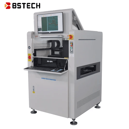
Bensun’s portfolio includes state-of-the-art AOI systems that cater to various needs within the PCB optical inspection domain. These systems utilize high-resolution cameras and sophisticated imaging technologies to ensure that every printed circuit board meets stringent quality standards. Additionally, their software solutions incorporate advanced algorithms for real-time data analysis, allowing manufacturers to detect defects early in the production process.
Bensun also provides customizable solutions that can be tailored to specific requirements in circuit board production. This flexibility ensures that whether you’re producing simple or complex PCBs, there are options available that will fit seamlessly into your existing workflow. With a focus on user-friendly interfaces and robust support services, Bensun makes it easy for manufacturers to adopt these advanced optical inspection technologies.
How Bensun Enhances PCB Manufacturing
Bensun enhances PCB manufacturing by significantly improving defect detection rates through its innovative optical inspection systems. By implementing their AOI technology, manufacturers can reduce rework and scrap rates associated with faulty printed circuit boards, ultimately leading to lower overall costs in circuit board production. This not only streamlines operations but also boosts confidence in product reliability among end-users.
Moreover, Bensun's commitment to continuous improvement means they regularly update their technology with the latest advancements in imaging and data analysis techniques. This proactive approach ensures that clients remain at the forefront of industry standards while maximizing efficiency across their PCB manufacturing processes. Additionally, their integration capabilities with Industry 4.0 initiatives empower manufacturers to leverage smart factory concepts for enhanced productivity.
Success Stories in Circuit Board Production
Numerous success stories highlight how companies have transformed their circuit board production lines by incorporating Bensun’s AOI solutions into their processes. One notable case involved a large electronics manufacturer who reported a 30% reduction in defect rates after integrating Bensun's advanced optical inspection system into their workflow for PCB assembly lines. This remarkable improvement not only saved costs but also enhanced customer satisfaction due to higher product quality.
Another client from the automotive sector experienced significant gains as well; they were able to increase throughput while maintaining rigorous quality control measures thanks to real-time feedback provided by Bensun's software algorithms during printed circuit board production inspections. These success stories underscore how effective pcb optical inspection can be when backed by reliable technology and expert support from industry leaders like Bensun.
Conclusion
As we wrap up our exploration of PCB optical inspection, it’s clear that this technology is not just a passing trend but a cornerstone of modern circuit board manufacturing. The future of optical inspection in PCB production is bright, with continuous advancements in imaging technologies and software algorithms that promise to enhance quality control further. As manufacturers strive for precision and efficiency, the role of automated optical inspection will only grow more critical in ensuring the reliability of printed circuit boards.
The Future of Optical Inspection in PCB
The future landscape of PCB optical inspection looks promising, driven by innovations such as artificial intelligence and machine learning. These technologies are set to revolutionize how we approach circuit board production by enabling real-time data analysis and adaptive learning capabilities. As the industry evolves, we can expect optical inspection systems to become even more sophisticated, seamlessly integrating into existing workflows while drastically improving defect detection rates.
Integrating AOI with Industry 4.0
Integrating automated optical inspection with Industry 4.0 principles presents an exciting opportunity for enhancing circuit board manufacturing processes. By connecting AOI systems to the Internet of Things (IoT), manufacturers can collect and analyze vast amounts of data from multiple sources, leading to smarter decision-making and predictive maintenance strategies. This synergy not only boosts efficiency but also ensures that every stage of printed circuit board production aligns with the highest standards for quality and performance.
Choosing the Right AOI Solutions for Your Needs
Selecting the right AOI solutions for your PCB manufacturing needs requires careful consideration of several factors including technology compatibility, scalability, and cost-effectiveness. It's essential to evaluate how different systems align with your specific requirements in circuit board production—whether that's high-speed inspections or intricate detail checks on complex designs. Ultimately, investing time in choosing an optimal solution will pay off through enhanced productivity and superior quality assurance in your PCB board production efforts.
