Introduction

In the fast-paced world of circuit board manufacturing, ensuring quality and precision is paramount. Automated optical inspection (AOI) has emerged as a game-changing technology in PCB manufacturing, offering a reliable solution to detect defects that could compromise performance. As the demand for high-quality PCBs increases, so does the importance of integrating advanced optical inspection systems into production lines.
Importance of Automated Optical Inspection
Automated optical inspection plays a crucial role in maintaining the integrity of PCB board manufacturing processes. By utilizing sophisticated imaging techniques, AOI systems can identify issues such as misalignments, solder defects, and component placement errors with remarkable accuracy. This level of scrutiny not only enhances product quality but also builds trust with clients reliant on flawless circuit board production.
Benefits in PCB Manufacturing
The benefits of implementing automated optical inspection in PCB manufacturing are substantial and multifaceted. First and foremost, AOI significantly reduces the likelihood of human error during inspections, leading to more consistent results across batches. Additionally, by catching defects early in the production process, manufacturers can save on costs associated with rework and scrap materials—ultimately boosting profitability.
Trends in Optical Inspection Technology
As technology evolves, so do the capabilities of automated optical inspection systems within PCB board production environments. Current trends include advancements in 3D inspection technologies that provide deeper insights into component integrity compared to traditional 2D methods. Furthermore, integration with artificial intelligence is set to revolutionize how automatic inspection systems learn from data over time, continuously improving their accuracy and efficiency.
Understanding Automated Optical Inspection

Automated Optical Inspection (AOI) is a revolutionary technology reshaping the landscape of circuit board manufacturing. This method employs sophisticated imaging techniques to detect defects and ensure quality in PCB production. By integrating automated optical inspection into their processes, manufacturers can significantly enhance the reliability and performance of their products.
Definition of Automated Optical Inspection
At its core, automated optical inspection refers to the use of cameras and software algorithms to examine printed circuit boards for defects. This process scans the surface of PCBs, identifying issues such as misalignment, soldering errors, or component placement inaccuracies. In essence, AOI acts as a vigilant guardian in circuit board production, ensuring that each unit meets stringent quality standards before it reaches consumers.
Key Components of Optical Inspection Systems
An effective optical inspection system comprises several key components that work together seamlessly. First and foremost is the camera system, which captures high-resolution images of the PCB surfaces during inspection. Coupled with advanced lighting systems—such as brightfield or darkfield illumination—these cameras can reveal minute details that would otherwise go unnoticed in PCB manufacturing processes.
Additionally, software plays a crucial role in analyzing the captured images for defects. This software utilizes complex algorithms to compare images against predefined templates or specifications, allowing for rapid identification of anomalies. Together with conveyor systems that transport PCBs through the inspection area, these components create an efficient workflow that enhances overall productivity in circuit board manufacturing.
How Automated Inspection Works
The operation of automated optical inspection systems is both sophisticated and efficient. Initially, a printed circuit board enters the AOI machine where it is positioned under high-resolution cameras equipped with advanced lighting techniques. As images are captured in real-time during this automatic inspection process, they are immediately sent to analysis software that scrutinizes each detail against established criteria specific to PCB board manufacturing standards.
Once potential defects are detected—be it misplaced components or insufficient solder—the system flags these anomalies for further review by operators or engineers. This combination of speed and precision not only minimizes human error but also streamlines production timelines significantly in PCB board production environments. Ultimately, automated optical inspection serves as an essential tool for maintaining quality assurance throughout every stage of circuit board production.
Advantages of Optical Inspection in PCB Production
Automated optical inspection (AOI) has revolutionized the landscape of PCB manufacturing, offering numerous advantages that enhance the overall production process. By leveraging advanced technologies, manufacturers can achieve higher accuracy, reduce costs, and minimize human error during circuit board production. This section delves into the key benefits of optical inspection systems in the realm of PCB board manufacturing.
Enhanced Accuracy and Consistency
One of the standout advantages of automated optical inspection is its ability to deliver enhanced accuracy and consistency across various stages of PCB manufacturing. Unlike manual inspections that can be prone to oversight, AOI systems utilize high-resolution cameras and sophisticated algorithms to detect even the tiniest defects on circuit boards. This level of precision not only ensures that each PCB board meets stringent quality standards but also fosters greater confidence among manufacturers in their production processes.
Moreover, consistency is a hallmark benefit when employing optical inspection technology; machines perform inspections uniformly without fatigue or variance over time. This leads to a more reliable output in circuit board production where adherence to specifications is paramount for performance and safety. Consequently, manufacturers can maintain tighter tolerances and produce higher-quality products with confidence.
Cost-Effectiveness in Circuit Board Manufacturing
In an industry where margins can be razor-thin, cost-effectiveness is crucial for success in PCB manufacturing. Automated optical inspection systems significantly reduce operational costs by streamlining processes that would otherwise require extensive labor hours for manual checks. With AOI technology handling inspections swiftly and accurately, manufacturers can allocate resources more efficiently—ultimately leading to lower overall production costs.
Additionally, by identifying defects early in the manufacturing process through automatic inspection techniques, companies can avoid costly rework or scrap later on. This proactive approach not only saves money but also enhances productivity by keeping assembly lines moving smoothly without interruptions due to quality issues. As a result, businesses engaged in circuit board production find themselves better positioned financially while maintaining high standards.
Reduction of Human Error
Human error remains one of the biggest challenges faced during circuit board production; however, automated optical inspection effectively mitigates this risk through its advanced capabilities. By replacing manual checks with automated systems designed specifically for precise detection tasks, manufacturers greatly minimize mistakes that could arise from fatigue or oversight among operators during lengthy inspections.
The reduction of human error translates directly into fewer defective products reaching customers—an essential factor for maintaining brand reputation and customer satisfaction in PCB board manufacturing sectors. Furthermore, this shift towards automation allows skilled workers to focus on more complex tasks rather than repetitive checking processes, enhancing workforce efficiency overall while simultaneously boosting morale within teams.
Types of Automated Optical Inspection Systems

In the realm of automated optical inspection, various systems cater to different needs and capabilities within the PCB manufacturing process. Understanding these types can help manufacturers choose the right technology for their specific circuit board production requirements. Let's dive into the main categories: 2D vs 3D inspection technologies, inline automated inspection, and offline automated optical inspection.
2D vs 3D Inspection Technologies
When it comes to optical inspection, one of the primary distinctions is between 2D and 3D technologies. Two-dimensional inspection relies on capturing images from a flat perspective, making it effective for detecting surface defects such as soldering errors or component misalignments in circuit board manufacturing. In contrast, three-dimensional inspection provides depth perception, allowing for a more comprehensive analysis that identifies issues like height discrepancies or shadowing effects in PCB board manufacturing.
The choice between these two technologies often hinges on the complexity of the boards being produced. For simpler designs, 2D systems may suffice; however, as circuit board production becomes more intricate with multi-layered assemblies and fine-pitch components, 3D systems prove invaluable. Ultimately, both methods play crucial roles in ensuring quality control during PCB manufacturing.
Inline Automated Inspection
Inline automated inspection integrates seamlessly into existing production lines for real-time monitoring during circuit board production. This system continuously checks each PCB as it moves through various stages of assembly, allowing for immediate feedback and corrections if defects are detected. By incorporating inline optical inspection technology, manufacturers can significantly reduce waste and rework costs associated with faulty boards.
One of the standout benefits of inline systems is their ability to maintain high throughput without sacrificing quality assurance in PCB board manufacturing processes. As each unit is inspected on-the-fly, operators can address issues promptly rather than discovering them later in post-production checks—this leads to enhanced efficiency overall. Inline automated optical inspection also allows manufacturers to gather valuable data about their production processes that can inform future improvements.
Offline Automated Optical Inspection
On the flip side of inline systems lies offline automated optical inspection, which operates independently from the main assembly line once batches are completed or at designated checkpoints during production runs. This method allows for more thorough inspections without impacting overall workflow since boards are removed from production temporarily for detailed examination using advanced imaging techniques. Offline inspections are particularly useful when validating complex assemblies or when transitioning between different product lines in circuit board manufacturing.
While offline systems may not provide real-time feedback like their inline counterparts, they offer a comprehensive analysis that ensures every aspect of quality control is met before products reach customers or end-users in PCB board manufacturing sectors. Moreover, these systems can be equipped with sophisticated algorithms that enhance defect detection capabilities beyond what might be feasible during fast-paced inline inspections—making them ideal for high-stakes applications where precision is paramount.
Leading Brands in Optical Inspection Technology

In the realm of automated optical inspection, several brands stand out for their innovative contributions and commitment to enhancing quality in circuit board manufacturing. These companies are at the forefront of developing cutting-edge technologies that ensure precision and reliability in PCB board production. Understanding their roles provides insight into how automated inspection can significantly improve the overall efficiency of PCB manufacturing processes.
Bensun Technology Overview
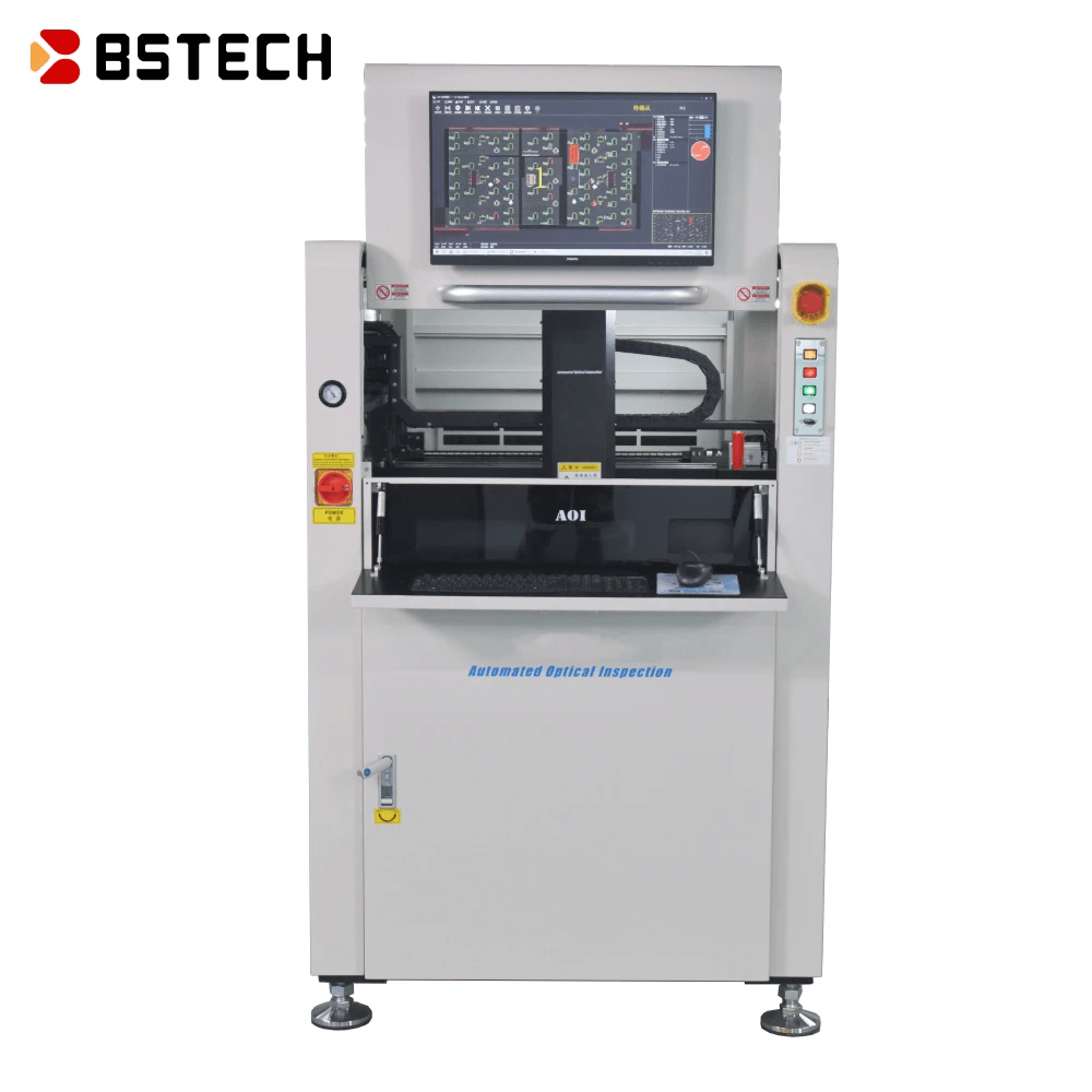
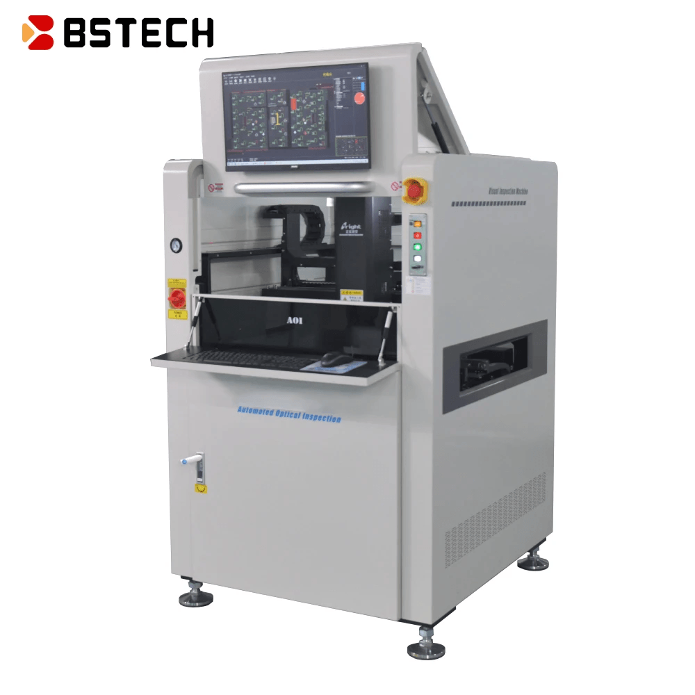
Bensun Technology has carved a niche for itself in the field of automated optical inspection, offering state-of-the-art solutions tailored for circuit board production. Their systems are designed to enhance accuracy and reduce defects during the PCB manufacturing process, making them a preferred choice among manufacturers seeking to streamline operations. With a focus on innovation, Bensun integrates advanced imaging technologies that provide real-time feedback during automatic inspection, ensuring that every circuit board meets stringent quality standards.
JUKI's Role in Automated Inspection
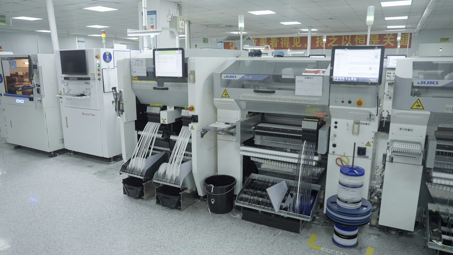
JUKI is another key player in the automated optical inspection landscape, renowned for its comprehensive solutions aimed at improving efficiency in PCB board manufacturing. The company’s systems leverage sophisticated algorithms and high-resolution cameras to detect even the minutest defects during circuit board production. By incorporating JUKI’s technology into their workflows, manufacturers can achieve higher throughput while maintaining exceptional quality control through effective automated inspection practices.
Comparison with Competitors
When comparing leading brands like Bensun and JUKI with their competitors, several factors come into play: technology sophistication, customer support, and adaptability to various manufacturing environments. While Bensun excels in providing tailored solutions with robust imaging capabilities for specific needs, JUKI offers a broader range of integrated systems suitable for high-volume production lines. Ultimately, choosing between these brands hinges on unique operational requirements within PCB manufacturing; however, both continue to push boundaries in automated optical inspection excellence.
The Future of Automated Optical Inspection
The landscape of automated optical inspection is evolving at a breakneck pace, driven by technological advancements and the increasing demand for precision in circuit board manufacturing. As the industry adapts to more complex designs and tighter tolerances, innovations on the horizon promise to enhance the capabilities of optical inspection systems significantly. From improved imaging techniques to faster processing speeds, these advancements will redefine what’s possible in PCB board production.
Innovations on the Horizon
One of the most exciting innovations in automated optical inspection is the development of high-resolution imaging systems that can detect even minute defects on circuit boards. These new systems leverage advanced optics and sensor technologies to provide unparalleled clarity and detail, ensuring that no flaw goes unnoticed during PCB manufacturing. Additionally, automation in lighting techniques is enhancing contrast and visibility, further improving defect detection rates.
Furthermore, as manufacturers strive for greater efficiency in PCB board production, innovations such as smart cameras equipped with real-time analytics are emerging. These intelligent devices can autonomously adjust their parameters based on environmental conditions or specific inspection requirements, leading to more accurate results with minimal human intervention. With these innovations, automated optical inspection is set to become an indispensable part of modern circuit board production.
Integration with AI and Machine Learning
The integration of artificial intelligence (AI) and machine learning into automated optical inspection systems marks a transformative step forward for quality assurance in circuit board manufacturing. By employing algorithms that learn from previous inspections, these systems can identify patterns associated with defects more effectively than traditional methods. This capability not only enhances defect detection but also reduces false positives, allowing for smoother operations during PCB manufacturing.
Moreover, AI-driven analytics can predict potential issues before they arise by analyzing historical data from past inspections. This predictive maintenance approach minimizes downtime and optimizes production processes in PCB board production facilities. As AI continues to evolve within automated optical inspection frameworks, we can expect a future where quality control becomes increasingly proactive rather than reactive.
Impact on PCB Board Production Efficiency
The impact of advancements in automated optical inspection technology on PCB board production efficiency cannot be overstated. With faster processing times and enhanced accuracy from cutting-edge systems, manufacturers are able to significantly reduce cycle times without compromising quality standards. This increased efficiency translates directly into cost savings across multiple facets of circuit board manufacturing.
Additionally, as automatic inspection processes become more streamlined through integration with other manufacturing technologies—such as robotics—overall workflow optimization becomes achievable. Manufacturers are not only able to keep up with rising demand but also improve their competitive edge within the market due to reduced lead times and higher output rates in PCB board production facilities. The future certainly looks bright for those embracing these innovations!
Conclusion
In summary, automated optical inspection (AOI) is a game-changer in the realm of circuit board manufacturing. The benefits of optical inspection extend beyond mere accuracy; they encompass cost savings, reduced human error, and overall enhanced efficiency in PCB production processes. As the industry continues to evolve, the role of automated inspection will only become more significant.
Recap of Optical Inspection Benefits
The advantages of optical inspection are manifold, particularly in PCB manufacturing where precision is paramount. Enhanced accuracy and consistency lead to fewer defects, which in turn reduces costs associated with rework and waste during circuit board production. Moreover, automated optical inspection systems significantly mitigate human error, allowing manufacturers to rely on technology for consistent quality assurance.
The Role of Automated Inspection in Quality Control
Automated inspection plays a crucial role in maintaining high standards within quality control processes for PCB board manufacturing. By integrating AOI into production lines, manufacturers can swiftly identify defects that may compromise product integrity before they escalate into costly issues. This proactive approach not only enhances the reliability of circuit boards but also builds customer trust through consistent delivery of high-quality products.
Future Trends in Circuit Board Manufacturing
Looking ahead, the future trends in circuit board manufacturing point towards even greater integration of advanced technologies like artificial intelligence and machine learning with automated optical inspection systems. These innovations promise to streamline processes further and enhance decision-making capabilities within PCB board production environments. As manufacturers adapt to these changes, we can expect a notable increase in efficiency and productivity across the entire sector.
