Introduction

In the fast-paced world of PCB manufacturing, ensuring quality and efficiency is paramount. One of the most significant advancements in this domain is the implementation of Automated Optical Inspection (AOI) technology. By harnessing the power of AOI machines, manufacturers can achieve unparalleled precision in their production processes, particularly when it comes to critical components like solder paste.
Understanding AOI in PCB Manufacturing
Automated Optical Inspection (AOI) has revolutionized how PCBs are inspected during manufacturing. This cutting-edge technology employs sophisticated cameras and algorithms to detect defects that may be invisible to the naked eye, making it an essential tool for quality assurance. With AOI inspection, manufacturers can swiftly identify issues related to solder paste application and other visual quality parameters before they escalate into costly problems.
Importance of Automated Inspection Technologies
The importance of automated inspection technologies cannot be overstated in today's competitive landscape. As products become more complex, the need for reliable and efficient inspection methods grows exponentially; manual inspections simply can't keep up with modern demands. Automated inspection not only enhances accuracy but also significantly reduces production time, allowing companies to deliver high-quality PCBs faster than ever before.
The Role of Bensun Technology
Bensun Technology stands at the forefront of this transformation with its innovative solutions tailored for PCB manufacturing needs. By offering state-of-the-art AOI machines equipped with advanced features such as solder paste inspection capabilities, Bensun ensures that manufacturers can maintain stringent quality standards without sacrificing efficiency. Partnering with Bensun Technology means investing in a future where automated optical inspection becomes synonymous with excellence in PCB production.
What is Automated Optical Inspection?
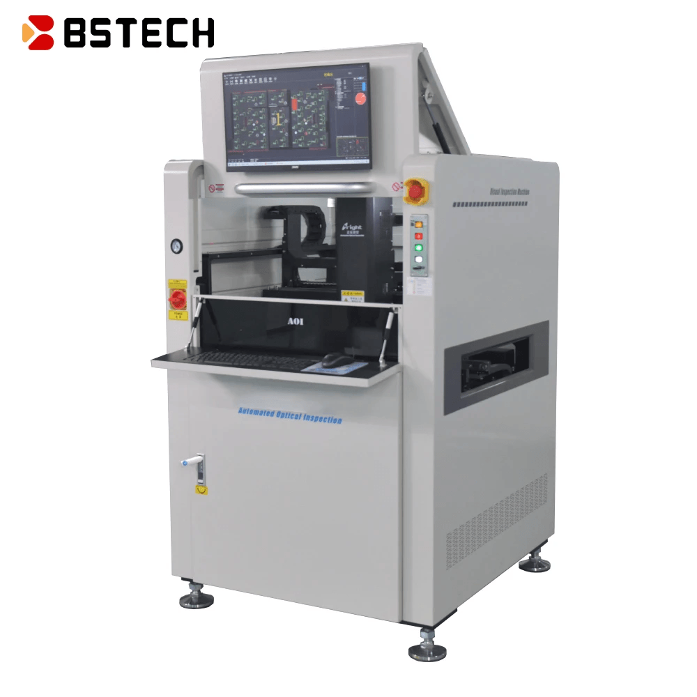
Automated Optical Inspection (AOI) represents a significant leap forward in the quality assurance processes of PCB manufacturing. This technology employs sophisticated imaging systems to detect defects and ensure that each component is correctly placed and soldered, thereby enhancing the overall reliability of electronic devices. By integrating an AOI machine into production lines, manufacturers can achieve higher levels of precision and efficiency.
Definition of AOI Technology
At its core, AOI technology involves the use of advanced cameras and software algorithms to conduct automatic inspection of printed circuit boards (PCBs). This process allows for rapid evaluation of visual quality by comparing captured images against predefined standards or templates. By employing automated optical inspection techniques, manufacturers can identify issues such as misalignments, missing components, or poor solder paste application much faster than traditional manual methods.
How AOI Machines Function
AOI machines operate by scanning PCBs with high-resolution cameras that capture detailed images from various angles. Once the images are acquired, specialized software analyzes them in real-time to detect any discrepancies from expected patterns or specifications. This automatic inspection process not only speeds up quality control but also reduces the chances of human error that can occur during manual inspections.
Benefits of AOI in PCB Manufacturing
The benefits of implementing automated optical inspection in PCB manufacturing are manifold. Firstly, it significantly enhances defect detection rates, allowing for early identification of potential issues before they escalate into larger problems down the line. Additionally, using an AOI machine leads to improved efficiency by streamlining workflows and reducing labor costs associated with manual inspections while maintaining high standards for solder paste inspection and overall product quality.
The Evolution of Inspection Techniques

The world of inspection techniques has undergone a remarkable transformation over the decades, particularly in the realm of PCB manufacturing. From rudimentary visual checks to sophisticated automated optical inspection (AOI) systems, the journey reflects technological advancements that have significantly enhanced quality control processes. This evolution not only improves efficiency but also ensures that products meet stringent quality standards.
Historical Overview of Inspection Methods
In the early days of PCB manufacturing, inspection was a labor-intensive process dominated by manual checks and visual inspections. Technicians would painstakingly examine each board for defects, relying on their keen eyesight and experience to catch issues like misaligned components or solder paste inconsistencies. While these methods were effective in their time, they were also prone to human error and could be exceedingly slow—qualities that are less than ideal in today's fast-paced production environments.
As technology began to evolve, so did the methods used for inspection. The introduction of basic electronic testing equipment marked a significant shift from purely manual methods to more automated solutions. However, it wasn't until the advent of AOI machines that manufacturers could truly revolutionize their quality assurance processes by incorporating advanced optical inspection technologies into their workflows.
Transition from Manual to Automated Inspection
The transition from manual inspections to automated inspection systems was driven by the need for greater accuracy and efficiency in PCB manufacturing. With increased complexity in designs and higher production volumes, relying solely on human inspectors became untenable; hence, companies began investing in automatic inspection systems like AOI machines. These machines use high-resolution cameras and sophisticated algorithms to detect defects with unparalleled precision—far exceeding what human inspectors could achieve.
Automated optical inspection (AOI) not only speeds up the process but also minimizes errors associated with fatigue or oversight during manual checks. Solder paste inspection is one area where this transition has proven particularly beneficial; AOI systems can quickly assess solder paste application quality across multiple boards without compromising accuracy or consistency. This shift has led many manufacturers to adopt AOI technology as a standard practice rather than an optional add-on.
The Impact of Technology on Quality Control
The impact of technology on quality control cannot be overstated; it has fundamentally changed how PCBs are inspected and verified for defects before reaching consumers. Automated optical inspection provides real-time feedback during production runs, allowing immediate corrective actions if any issues arise—something that was nearly impossible with traditional methods. Consequently, this leads to improved product reliability and customer satisfaction as fewer defective boards make it through the pipeline.
Moreover, integrating advanced features into AOI machines enables even deeper insights into manufacturing processes through data analytics capabilities related to solder paste application and overall product integrity analysis. As manufacturers embrace these technologies fully, they find themselves not just keeping pace with industry standards but setting them instead—creating a ripple effect throughout supply chains focused on enhanced efficiency and reduced waste rates across operations globally.
Types of AOI Inspection

Automated Optical Inspection (AOI) has revolutionized the way we ensure quality in PCB manufacturing. By employing various types of inspection, manufacturers can detect defects early in the production process, reducing waste and improving efficiency. In this section, we will explore three key types of AOI inspection: optical inspection for visual quality, solder paste inspection, and advanced features of automated optical inspection.
Optical Inspection for Visual Quality
Optical inspection is a cornerstone of automated optical inspection systems, leveraging high-resolution cameras to capture detailed images of PCB surfaces. This type of inspection enables the detection of physical defects such as scratches, misalignments, and component placement errors that could compromise the integrity of the circuit board. By integrating an AOI machine into the production line, manufacturers can significantly improve visual quality assurance while minimizing human error.
The benefits of optical inspection extend beyond mere defect detection; they also enhance overall process efficiency. With automatic inspections conducted at high speeds, manufacturers can keep pace with rapid production demands without sacrificing quality. This not only boosts productivity but also instills confidence in end-users regarding the reliability and performance of their PCBs.
Moreover, advancements in optical technology allow for multi-angle inspections and 3D imaging capabilities, which provide a comprehensive view of each PCB's condition. These features enable more thorough assessments than traditional methods could offer. As a result, optical inspection remains an essential component in any effective AOI strategy.
Solder Paste Inspection: Ensuring Proper Application
Solder paste plays a critical role in PCB assembly by providing the necessary connections between components and circuit boards. Solder paste inspection is vital to ensure that it is applied correctly—too much or too little can lead to electrical failures or manufacturing defects down the line. An efficient AOI machine specifically designed for solder paste inspections identifies issues such as insufficient volume or improper placement before they become costly problems.
During this type of automated inspection process, high-resolution cameras scrutinize solder paste deposits on each pad to verify their dimensions and locations accurately. The ability to conduct real-time evaluations allows manufacturers to make immediate adjustments if discrepancies are detected—ensuring optimal soldering conditions before components are placed on PCBs. Consequently, this proactive approach minimizes rework costs and enhances overall production reliability.
Furthermore, integrating solder paste inspections into your automated optical inspection routine can lead to significant improvements in yield rates and product quality over time. By catching potential issues early on with precise measurements provided by advanced AOI systems, companies can reduce waste associated with faulty assemblies while ensuring that every board meets stringent industry standards.
Advanced Features of Automated Optical Inspection
The landscape of automated optical inspection is constantly evolving with cutting-edge technology that enhances its capabilities beyond basic defect detection. Modern AOI machines come equipped with advanced features like artificial intelligence (AI) algorithms that analyze data patterns from previous inspections to improve accuracy continuously over time. These smart systems learn from past errors and adapt their criteria accordingly—making them invaluable assets in any high-volume manufacturing environment.
In addition to AI integration, many automated optical inspections now utilize 3D imaging techniques that allow for more detailed assessments than traditional 2D methods could provide alone. This depth perception helps identify hidden defects beneath components or irregularities on complex surfaces—crucial factors often overlooked during standard checks but vital for ensuring long-term performance stability in PCBs.
Lastly, enhanced reporting tools accompany these advanced features by offering real-time feedback dashboards showcasing live data analytics from ongoing inspections across multiple lines simultaneously—a game-changer when it comes to optimizing workflow processes! With these sophisticated functionalities at their disposal through an integrated AOI system like those offered by Bensun Technology; manufacturers are better equipped than ever before to maintain superior quality control throughout every stage of production while maximizing operational efficiency.
The Significance of Solder Paste Inspection
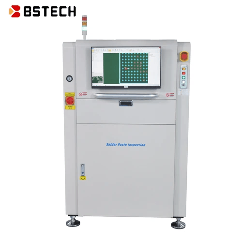
Solder paste inspection is a critical aspect of PCB manufacturing, ensuring that the application of solder paste meets stringent quality standards. Solder paste acts as a bridge between electronic components and the circuit board, making its proper application essential for reliable electrical connections. Without effective inspection, defects can lead to costly failures in electronic devices, underscoring the importance of automated optical inspection (AOI) in this process.
The Role of Solder Paste in PCBs
Solder paste is a viscous mixture of powdered solder and flux, applied to printed circuit boards (PCBs) to facilitate the attachment of components during assembly. Its role cannot be overstated; it ensures that components are securely bonded to the PCB while providing necessary electrical conductivity. An improper solder paste application can result in weak joints or shorts, which can compromise device functionality and longevity.
How AOI Inspects Solder Paste Quality
Automated Optical Inspection (AOI) machines are designed to meticulously examine solder paste quality on PCBs by capturing high-resolution images and analyzing them for defects. These machines utilize advanced algorithms and optical inspection techniques to assess parameters such as volume, placement accuracy, and even thickness of the solder paste deposits. By employing AOI inspection systems, manufacturers can detect inconsistencies early in the production process, allowing for immediate corrective actions before moving forward.
Consequences of Poor Solder Paste Inspection
Neglecting proper solder paste inspection can have severe repercussions for manufacturers and consumers alike. Defective solder joints may lead to intermittent connections or complete failures in electronic devices, resulting in costly recalls or repairs that tarnish brand reputation. Moreover, poor quality control stemming from inadequate automated inspection processes can ultimately affect customer satisfaction and trust—something no company wants to risk.
Integrating AOI in PCB Production Lines
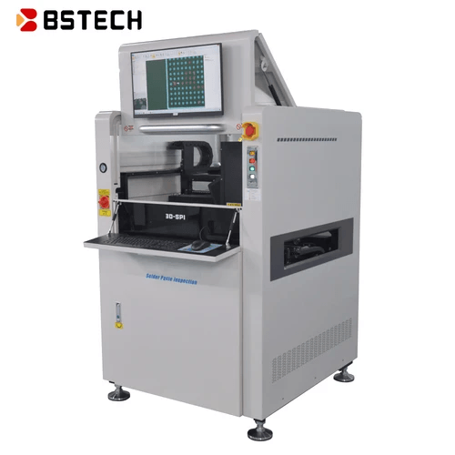
Integrating Automated Optical Inspection (AOI) systems into PCB production lines is a game changer for manufacturers aiming to enhance quality control. The shift towards automated inspection reduces human error while increasing efficiency, enabling companies to maintain high standards without sacrificing speed. With the right AOI machine in place, manufacturers can ensure that every component meets stringent quality requirements.
The Process of Implementing AOI Systems
Implementing an AOI system involves several crucial steps that start with assessing the specific needs of the production line. Manufacturers must evaluate their current processes and determine where automated inspection can provide the most benefit, particularly in areas like solder paste inspection and optical inspection. After identifying these needs, selecting the appropriate AOI machine tailored for those requirements is essential for seamless integration.
Once the right equipment is chosen, training staff on how to operate and maintain the AOI machine becomes necessary to maximize its potential. This includes understanding how automated optical inspection works and familiarizing them with troubleshooting common issues that may arise during operation. Finally, continuous monitoring and adjustments will ensure that the system remains effective as production demands evolve over time.
Custom Solutions by Bensun Technology
Bensun Technology stands out by offering custom solutions tailored specifically for each client's unique production needs. Their expertise in automated inspection allows them to design AOI systems that not only fit seamlessly into existing workflows but also enhance overall performance through advanced features like real-time data analytics and adaptive learning capabilities. This level of customization ensures optimal solder paste inspection processes are achieved while maintaining top-notch quality standards.
Moreover, Bensun’s commitment to innovation means they stay ahead of industry trends, providing clients with cutting-edge technology that boosts productivity without compromising accuracy. Their team collaborates closely with clients throughout implementation, ensuring that every aspect—from software integration to hardware setup—is executed flawlessly. Ultimately, these bespoke solutions empower manufacturers to achieve a competitive edge in a rapidly evolving market.
Enhancements in Efficiency and Accuracy
The introduction of an AOI system significantly enhances efficiency across PCB production lines by automating repetitive tasks traditionally performed manually. With automated optical inspection taking center stage, manufacturers can increase throughput while reducing lead times—an essential factor in today’s fast-paced electronics market. Additionally, implementing an effective solder paste inspection process ensures that defects are caught early on, preventing costly rework or product failures down the line.
Accuracy is another critical area where AOI shines; these machines utilize advanced imaging technology to detect even the slightest discrepancies on PCBs—something human inspectors might miss under pressure or fatigue. This level of precision not only improves product reliability but also bolsters customer satisfaction as products consistently meet or exceed expectations. By integrating such robust automated inspection technologies into their operations, manufacturers can confidently deliver high-quality products while optimizing resource allocation.
Conclusion
In the fast-paced world of PCB manufacturing, the importance of automated inspection cannot be overstated. With the rise of technologies like AOI machines, companies can achieve unprecedented levels of quality control and efficiency. As we move forward, understanding and integrating these advancements will be crucial for staying competitive.
Future Trends in Automated Inspection
The future of automated inspection is bright and full of possibilities. Innovations in AI and machine learning are set to enhance AOI technology, allowing for even more sophisticated optical inspection capabilities. We can expect a shift towards more adaptive systems that learn from previous inspections, improving solder paste inspection accuracy over time while minimizing human intervention.
The Benefits of Partnering with Bensun Technology
Partnering with Bensun Technology offers manufacturers a unique edge in the realm of automated optical inspection. Their custom solutions ensure that each AOI machine is tailored to meet specific production needs, enhancing overall efficiency and accuracy. With Bensun's expertise in automatic inspection systems, businesses can rest assured they are leveraging cutting-edge technology to maintain high standards in PCB manufacturing.
Maximizing Quality with AOI in PCB Manufacturing
To truly maximize quality in PCB manufacturing, integrating automated optical inspection into production lines is essential. By employing advanced AOI techniques, companies can significantly reduce errors associated with manual inspections and ensure consistent solder paste application across all products. Ultimately, embracing these innovations not only elevates product quality but also enhances customer satisfaction and trust.
