Introduction

In the fast-paced world of PCB manufacturing, ensuring the quality of solder connections is paramount. This is where solder paste inspection comes into play, serving as a critical checkpoint in the production process. By utilizing advanced optical inspection technologies, manufacturers can detect issues early on, saving time and resources while maintaining high standards.
Understanding Solder Paste Inspection
Solder paste inspection refers to the process of examining the application of solder paste on printed circuit boards (PCBs) before components are placed during assembly. The main goal is to ensure that the right amount of solder paste is applied in the correct locations, which directly affects the reliability and performance of electronic devices. A thorough understanding of this process helps manufacturers avoid costly mistakes and enhances overall production efficiency.
Importance of Optical Inspection in PCB Manufacturing
Optical inspection plays a vital role in PCB manufacturing by providing a non-contact method to evaluate solder paste application quality. By employing sophisticated optical inspection machines, manufacturers can quickly identify defects such as insufficient or excessive solder paste deposits, which could lead to poor electrical connections or component failures. This proactive approach not only improves product quality but also boosts customer confidence in end products.
Overview of Inspection Technologies
The landscape of solder paste inspection technologies has evolved significantly with advancements in both 2D and 3D machine capabilities. While traditional methods offered basic visual assessments, modern optical inspection machines leverage high-resolution imaging and complex algorithms for more accurate evaluations. As we explore these various technologies throughout this discussion, it becomes clear that selecting the right equipment is essential for optimizing PCB production processes.
What is Solder Paste Inspection?

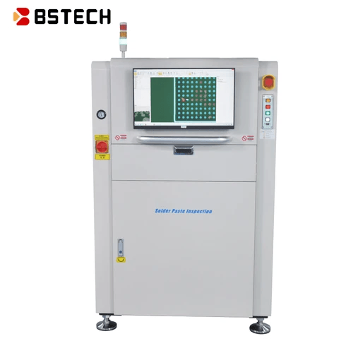
Solder paste inspection (SPI) is a critical step in the PCB manufacturing process, ensuring that solder paste is applied correctly before components are placed on the board. This inspection helps identify issues such as insufficient or excessive solder paste application, which can lead to defects in the final product. By utilizing advanced optical inspection technologies, manufacturers can enhance the reliability and quality of their PCB solder connections.
Definition and Purpose
At its core, solder paste inspection refers to the evaluation of the solder paste deposits on a printed circuit board (PCB) prior to component assembly. The primary purpose of SPI is to ensure that the right amount of solder paste is applied in precise locations for optimal connections during reflow soldering. This proactive approach minimizes potential defects and enhances overall production efficiency by catching problems early in the manufacturing process.
Key Benefits of Solder Paste Inspection
The advantages of implementing effective solder paste inspection are numerous and impactful for PCB manufacturers. Firstly, it significantly reduces defects caused by improper soldering, leading to higher yields and lower rework costs—an essential factor in maintaining profitability. Secondly, integrating SPI with optical inspection machines allows for real-time feedback during production, enabling immediate adjustments to be made when issues arise with solder flux application or other variables.
Another key benefit lies in improved traceability; detailed records from inspections can help identify trends over time and facilitate continuous improvement initiatives within manufacturing processes. Furthermore, using advanced 3D machines enhances depth perception during inspections and provides more accurate assessments than traditional 2D methods alone.
Common Challenges in Implementation
Despite its benefits, implementing effective solder paste inspection does come with challenges that manufacturers must navigate carefully. One common issue involves calibrating optical inspection machines accurately so that they can detect anomalies without generating false positives or negatives—striking a balance between sensitivity and specificity can be tricky.
Additionally, variations in different types of solder flux used across various applications may complicate inspections; not all fluxes behave similarly under optical scrutiny due to their unique properties and compositions. Lastly, training personnel to operate these sophisticated systems effectively requires time and investment—a hurdle many companies face as they strive for seamless integration into existing workflows.
The Role of Optical Inspection Machines

In the realm of PCB manufacturing, optical inspection machines play a pivotal role in ensuring quality control and reliability. These machines utilize advanced technologies to scrutinize solder paste application, detect defects, and ensure that solder flux is applied correctly. By integrating optical inspection into the production line, manufacturers can enhance their solder paste inspection processes significantly.
How Optical Inspection Works
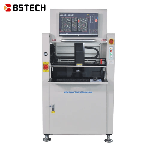
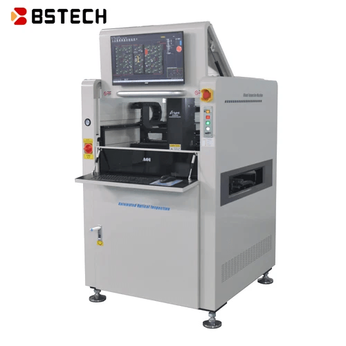
Optical inspection machines operate by capturing high-resolution images of the PCB surfaces where solder paste is applied. Using sophisticated algorithms, these machines analyze the images to identify inconsistencies in solder paste deposits and evaluate the presence of solder flux residues. The result is a detailed assessment that helps manufacturers maintain optimal standards during the PCB soldering process.
The core mechanism involves illuminating the surface with various light wavelengths, which allows for enhanced contrast and clarity in image capture. This technology not only detects issues like insufficient or excessive solder paste but also highlights potential alignment problems with components on the board. By leveraging this insight, manufacturers can make informed decisions to rectify any issues before proceeding further down the production line.
Integration with Solder Machines
Integrating optical inspection machines with solder machines creates a seamless workflow that enhances overall efficiency in PCB manufacturing. When these systems work together, they ensure that every layer of production is monitored for quality assurance—right from applying solder paste to placing components on PCBs. This synergy reduces human error and accelerates response times when defects are detected.
The integration also allows for real-time feedback loops; if an issue arises during inspection, adjustments can be made immediately on the solder machine to rectify it before it escalates into a larger problem. Furthermore, data collected from inspections can be used to optimize future processes by analyzing trends and recurring issues related to specific types of solder flux or paste application techniques. Thus, combining these technologies results in a more robust manufacturing process.
Benefits of 3D Optical Inspection
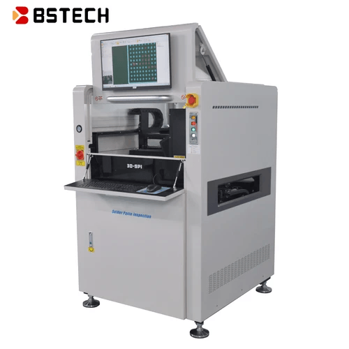
3D optical inspection takes traditional methods up a notch by providing depth perception and volumetric analysis of solder paste applications on PCBs. Unlike 2D inspections that may miss subtle variations in height or volume, 3D machines offer comprehensive insights into how well solder paste has been applied across different components on the board. This capability ensures that even minute discrepancies are caught early in the production cycle.
Additionally, 3D optical inspection enhances defect detection capabilities significantly by allowing for complete visualization of all angles around each component—something crucial for complex assemblies where space is limited and precision is key. It also aids in verifying whether sufficient amounts of solder flux have been utilized effectively during assembly processes, thereby reducing potential failures post-manufacturing due to inadequate connections or bridging issues between components.
In summary, employing 3D optical inspection as part of your overall strategy not only boosts quality assurance but also contributes positively to long-term cost savings through reduced rework rates and improved yield percentages from your PCB output.
Solder Flux and Its Importance

Solder flux plays a crucial role in the soldering process, influencing both the quality of the joint and the effectiveness of solder paste inspection. Understanding its types and applications can significantly enhance optical inspection results, ensuring that PCB assemblies meet stringent quality standards. In this section, we will delve into the various types of solder flux, their effects on inspection processes, and best practices for application.
Types of Solder Flux
Solder flux comes in several varieties, each designed for specific applications within PCB manufacturing. The most common types include rosin-based flux, water-soluble flux, and no-clean flux. Rosin-based flux is popular due to its excellent wetting properties but requires cleaning after soldering; water-soluble flux is effective but must be thoroughly cleaned to prevent corrosion; no-clean flux allows for minimal residue, making it ideal when post-soldering cleaning is impractical.
Understanding these types is essential for optimizing solder paste inspection processes since each type interacts differently with solder paste and can affect detection accuracy during optical inspection. For instance, residues from water-soluble flux can obscure defects during 3D machine inspections if not properly cleaned. Therefore, selecting the right type of solder flux based on your specific application needs can greatly enhance the reliability of your PCB solder joints.
Effects of Solder Flux on Inspection
The choice of solder flux directly impacts the efficiency and accuracy of optical inspection machines used in solder paste inspection. Contaminants left by certain types of flux can interfere with detection algorithms employed by 2D or 3D machines, leading to false positives or missed defects during inspections. Moreover, excessive residue may hinder proper adhesion between components and PCB pads, which could result in costly rework or failure rates.
In addition to affecting visual clarity during inspections, different solder fluxes also influence how well the optical inspection systems detect variations in paste volume or placement errors on PCBs. For example, a high-viscosity rosin-based flux may obscure small discrepancies that a more fluid no-clean option would reveal more readily under an optical inspection machine's lens. Thus, understanding these effects helps manufacturers make informed decisions about both their choice of materials and their approach to quality assurance.
Best Practices for Flux Application
To maximize the effectiveness of both solder paste and subsequent inspections, it's crucial to follow best practices when applying solder flux during manufacturing processes. First off, ensure uniform application across all areas where components will be placed; inconsistent coverage can lead to inadequate wetting or bonding issues that are difficult to catch during visual inspections later on. Utilizing automated dispensing systems can help achieve this uniformity while minimizing human error.
Additionally, always allow sufficient time for any solvents within the chosen type of solder flux to evaporate before proceeding with reflow or wave soldering processes; this not only improves joint integrity but also aids optical inspection by reducing residue interference on PCBs after assembly. Finally, conducting regular maintenance checks on your equipment ensures optimal performance from both your 3D machines and other optical inspection tools used throughout production.
Types of Solder Paste Inspection Methods

In the world of PCB manufacturing, ensuring the quality and reliability of solder joints is paramount. Solder paste inspection methods are crucial in identifying defects that could compromise electronic assemblies. These methods can be broadly categorized into automated inspection techniques and manual processes, each with its own set of advantages.
Automated Inspection Techniques
Automated inspection techniques are revolutionizing the way we approach solder paste inspection, leveraging advanced technology to enhance accuracy and efficiency. Optical inspection machines equipped with sophisticated algorithms can quickly analyze solder paste deposits on PCBs, identifying inconsistencies in thickness and placement. This not only speeds up the production process but also reduces human error associated with manual inspections, ensuring that every solder joint meets stringent quality standards.
Moreover, many automated systems utilize 3D machine capabilities to provide a comprehensive view of the solder paste application, allowing for a more detailed analysis than traditional 2D methods. These machines can detect issues related to solder flux application and ensure that the right amount is used for optimal results. By automating the inspection process, manufacturers can focus on scaling production while maintaining high-quality standards in their PCB solder applications.
Manual Inspection Processes
While automation is on the rise, manual inspection processes still play a vital role in certain scenarios within solder paste inspection. Trained technicians use visual assessments to evaluate solder paste deposits and flux application manually; this method allows for nuanced judgment that machines may overlook in complex situations. Manual inspections are often employed during initial production runs or when new products are introduced to ensure that everything aligns with specifications before fully transitioning to automated systems.
However, relying solely on manual processes can lead to inconsistencies due to human error or fatigue over time. It’s essential for manufacturers to strike a balance between manual oversight and automated solutions for optimal quality control in their PCB assembly lines. By integrating both approaches effectively, companies can enhance their overall efficiency while maintaining rigorous standards for solder paste quality.
Comparison of 2D and 3D Inspection
When it comes to comparing 2D and 3D inspection methods within solder paste inspection frameworks, both have unique strengths that cater to different needs in PCB manufacturing environments. Traditional 2D optical inspection machines capture images from one angle; they excel at detecting surface-level issues such as misalignment or insufficient coverage but may miss depth-related problems like insufficient volume of solder paste or improper flux distribution beneath components.
On the other hand, 3D optical inspection machines provide a multi-dimensional perspective on each deposit's height and volume—crucial factors when assessing whether enough solder has been applied or if there's an issue with the underlying substrate due to improper flux usage. This depth perception allows manufacturers not just to identify problems but also understand their root causes better than ever before.
In conclusion, while both techniques have their merits, opting for a robust combination of 2D for quick checks alongside advanced 3D capabilities offers an unparalleled level of assurance in achieving high-quality PCB assembly outcomes through effective solder paste inspection.
Choosing the Right Inspection Equipment
Selecting the right inspection equipment is crucial for ensuring high-quality solder paste inspection in PCB manufacturing. With various technologies available, understanding the features that enhance optical inspection and integrate seamlessly with solder machines is essential. This section will guide you through key considerations, reputable brands, and Bensun Technology Co., Ltd.'s unique offerings.
Features to Look for in Inspection Machines
When evaluating inspection machines for solder paste inspection, several features should be prioritized. First and foremost, look for advanced optical inspection capabilities that can accurately detect defects in solder paste application, such as insufficient volume or misalignment on PCB solder pads. Additionally, consider whether the machine offers 3D imaging; this technology provides a more comprehensive view of the solder paste layer compared to traditional 2D methods.
Another critical feature is integration capabilities with existing production lines and solder machines. An effective optical inspection machine should easily connect with your current setup without causing disruptions to your workflow. Finally, user-friendly software interfaces allow operators to quickly analyze results and make necessary adjustments based on real-time feedback from inspections.
Top Brands in Solder Paste Inspection
The market for solder paste inspection equipment boasts several top brands known for their reliability and innovation in optical inspection technology. Companies like Koh Young Technology are well-regarded for their advanced 3D measurement systems that ensure precise evaluation of solder paste application on PCBs. Another notable name is Viscom AG, which offers versatile solutions tailored to various manufacturing environments while maintaining high standards of quality assurance.
In addition to these industry leaders, other brands such as Omron and Saki Corporation provide robust options that cater to different production needs and budgets. These companies consistently invest in research and development to enhance their optical inspection machines' capabilities while addressing common challenges faced during implementation of solder flux applications.
Bensun Technology Co., Ltd. Solutions
Bensun Technology Co., Ltd. stands out as a provider of cutting-edge solutions designed specifically for effective solder paste inspection processes within PCB manufacturing environments. Their optical inspection machines incorporate state-of-the-art technology that ensures accurate detection of defects related to both solder flux application and overall quality control measures on PCBs.
By offering customizable solutions tailored to clients' unique needs, Bensun enables manufacturers to optimize their production processes while minimizing waste associated with improper solder paste applications or misaligned components on PCBs. Furthermore, Bensun's commitment to customer support ensures clients receive ongoing assistance throughout their journey toward enhanced quality assurance practices using advanced 3D machine technology.
Conclusion
In the fast-paced world of PCB manufacturing, solder paste inspection stands as a critical quality control measure. By ensuring that solder paste is applied accurately and uniformly, manufacturers can avoid costly defects and improve overall product reliability. The integration of advanced optical inspection technologies enhances this process, making it more efficient and effective than ever before.
Key Takeaways on Solder Paste Inspection
Solder paste inspection is essential for maintaining high standards in PCB soldering processes. It not only helps in identifying potential issues early on but also contributes to reducing waste and rework costs associated with faulty solder joints. Understanding the role of solder flux and its interaction with various inspection technologies can significantly enhance the effectiveness of any production line.
Future Trends in Optical Inspection Technology
The future of optical inspection technology looks promising, with trends pointing towards increased automation and integration of artificial intelligence. As 3D machines become more prevalent, they will offer deeper insights into the quality of solder paste application, allowing for real-time adjustments during the manufacturing process. Additionally, advancements in machine learning will enable optical inspection machines to adapt and learn from previous inspections, further improving accuracy over time.
How Bensun Can Enhance Your Production Process
Bensun Technology Co., Ltd. offers cutting-edge solutions tailored to meet the challenges of modern PCB manufacturing through superior solder paste inspection equipment. Their range includes state-of-the-art optical inspection machines designed to work seamlessly with existing solder machines while providing comprehensive analysis capabilities. By choosing Bensun’s solutions, manufacturers can expect enhanced efficiency, reduced error rates, and ultimately a more robust production process.
