Introduction
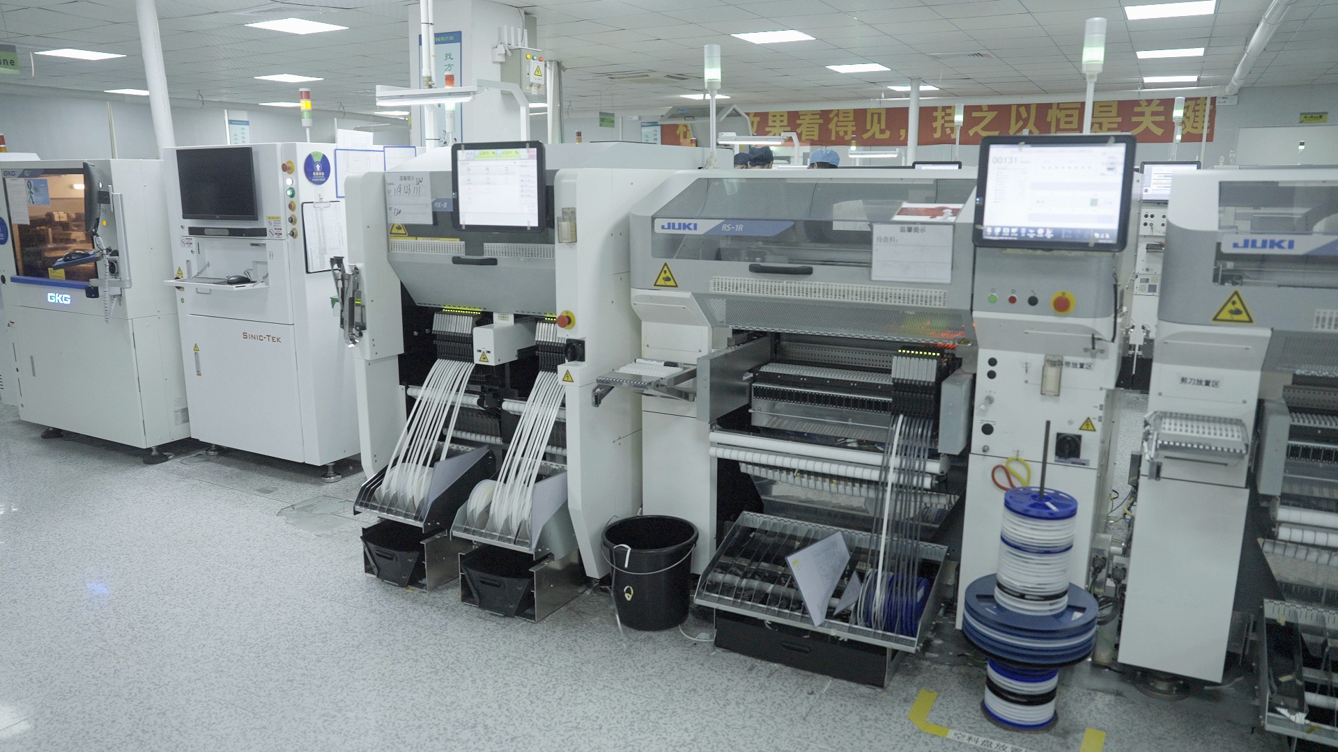
In the fast-paced world of electronic manufacturing, maintaining high-quality standards is crucial for success. One of the most effective methods for ensuring quality in printed circuit board (PCB) production is Automated Optical Inspection (AOI). This technology not only enhances the accuracy of inspections but also plays a pivotal role in streamlining processes and reducing defects.
Understanding AOI in PCB Manufacturing
Automated Optical Inspection (AOI) refers to the use of machine vision systems to detect defects and ensure quality during PCB manufacturing. By employing advanced optical inspection techniques, AOI allows manufacturers to identify issues such as misalignment, solder defects, and component placement errors with remarkable precision. This proactive approach helps maintain high standards throughout the production process, ultimately leading to superior products.
The Role of AOI in Quality Control
Quality control is a fundamental aspect of electronic manufacturing, and AOI inspection serves as a powerful tool in this regard. By integrating automated inspection into their workflows, manufacturers can significantly reduce human error while increasing inspection speed and reliability. This not only ensures that each PCB meets stringent quality requirements but also enhances overall operational efficiency.
Benefits of Automated Optical Inspection
The benefits of automated optical inspection are numerous and impactful for any organization involved in electronics production. Firstly, it vastly improves defect detection rates compared to manual inspection methods, leading to higher yields and lower rework costs. Additionally, AOI systems can be customized for specific applications like solder paste inspection or other vision inspection techniques, providing flexibility that manual processes simply cannot match.
What Is Automated Optical Inspection

Automated Optical Inspection (AOI) is a crucial technology in the realm of electronic manufacturing, specifically designed to enhance quality control processes. By utilizing advanced machine vision systems, AOI inspection identifies defects in printed circuit boards (PCBs) and other electronic components with remarkable precision. This automated inspection method not only increases efficiency but also significantly reduces the likelihood of human error during quality checks.
Definition of AOI in Electronics
In electronics, AOI refers to the process of using optical inspection techniques to automatically detect defects on PCBs and assemblies. It employs high-resolution cameras and sophisticated algorithms to analyze images of components, solder joints, and traces on a board. The primary goal is to ensure that each product meets stringent quality standards before it moves further along the production line.
How AOI Inspection Works
AOI inspection operates by capturing images of PCBs at various stages of production, particularly after solder paste application and component placement. These images are then analyzed using powerful software that compares them against predefined criteria or templates for accuracy. If discrepancies are detected—whether it’s a misaligned component or insufficient solder—the system flags these issues for review, ensuring that only defect-free products reach consumers.
Differences Between AOI and Manual Inspection
When comparing automated inspection methods like AOI with manual inspection practices, several key differences emerge. Firstly, while manual inspections rely heavily on human observation—which can be subjective and prone to errors—AOI provides consistent results through objective analysis powered by machine vision systems. Additionally, automated optical inspection is significantly faster than manual checks; it can process thousands of components per hour compared to a few dozen inspected by hand, making it an indispensable tool in modern electronic manufacturing environments.
Types of Optical Inspections
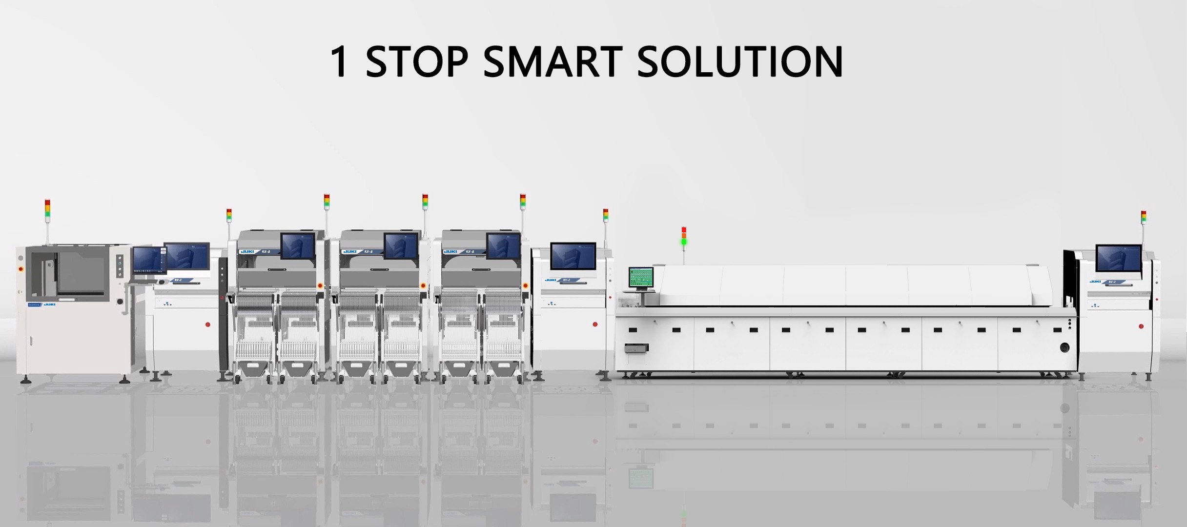
In the realm of electronic manufacturing, optical inspection techniques are pivotal for ensuring product quality and reliability. Various types of inspections, including solder paste inspection and machine vision systems, play a crucial role in maintaining high standards. Understanding these methods can significantly enhance the efficiency and accuracy of automated inspection processes.
Solder Paste Inspection Explained
Solder paste inspection (SPI) is a specialized form of optical inspection that focuses on assessing the application of solder paste on printed circuit boards (PCBs). This step is critical because improper solder paste application can lead to defects in the final assembly, affecting overall performance. By employing AOI inspection techniques during this phase, manufacturers can identify issues like insufficient or excessive solder paste before they escalate into more significant problems.
During solder paste inspection, advanced machine vision systems capture detailed images of the PCB surface to analyze the volume and placement of solder paste deposits. These systems utilize sophisticated algorithms to ensure that every aspect meets predefined specifications, thereby enhancing quality control measures. By integrating SPI into their production lines, manufacturers can significantly reduce defects and improve yield rates.
Role of Machine Vision Systems
Machine vision systems are at the heart of modern optical inspections, providing unmatched accuracy and speed in identifying potential defects during electronic manufacturing processes. These automated inspection solutions utilize high-resolution cameras combined with powerful software to analyze images in real-time, making them indispensable for maintaining quality standards. The ability to perform thorough inspections without human intervention minimizes errors associated with manual inspections while increasing overall productivity.
The versatility of machine vision systems allows them to adapt to various types of inspections beyond just AOI; they can be configured for tasks such as component placement verification and post-reflow inspections as well. This flexibility ensures that manufacturers can tailor their automated inspection processes according to specific production requirements without compromising quality or efficiency. As technology continues to evolve, these systems will become even more integral to achieving optimal results in electronic manufacturing.
Vision Inspection Techniques
Vision inspection techniques encompass a wide range of methodologies designed for detecting defects within PCBs effectively. These techniques include both 2D and 3D imaging capabilities that enhance detection rates for various flaws such as misalignments or missing components during production runs. By leveraging advanced algorithms alongside high-resolution imaging technologies, automated optical inspections provide reliable assessments that traditional manual methods simply cannot match.
One notable advantage of utilizing vision inspection techniques is their ability to perform consistent evaluations across large batches without fatigue or variance in judgment—common pitfalls in manual inspections. Furthermore, these methods facilitate rapid feedback loops within production lines; when a defect is detected through AOI inspection or other means, adjustments can be made almost immediately to rectify issues before they propagate further down the line. This proactive approach not only saves time but also significantly reduces waste while ensuring higher-quality end products.
The Importance of AOI in Electronic Manufacturing
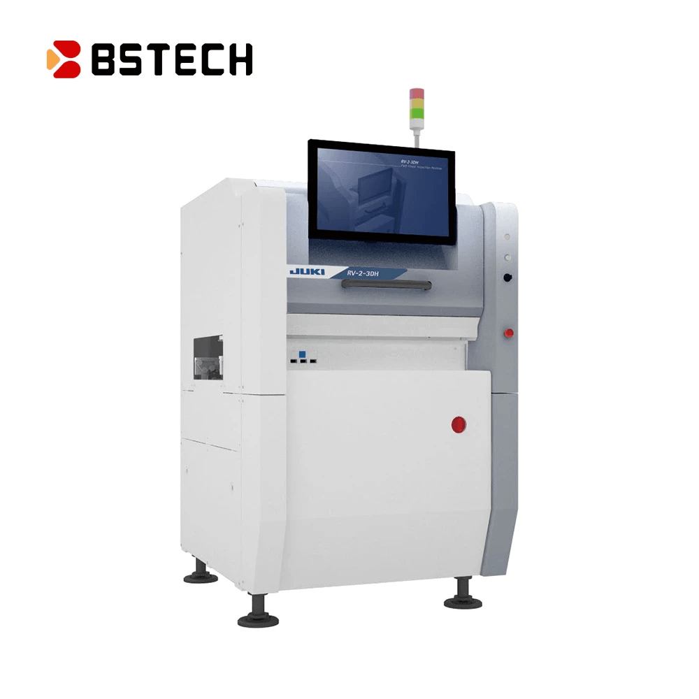
Automated Optical Inspection (AOI) plays a pivotal role in ensuring the quality and reliability of PCB production in electronic manufacturing. By employing machine vision systems, AOI inspection methods can quickly and accurately identify defects that might be missed by manual inspection processes. This not only streamlines the quality control process but also enhances overall production efficiency.
Ensuring Quality in PCB Production
Quality assurance is paramount in PCB production, where even the smallest defect can lead to significant failures down the line. AOI inspection provides a robust solution by utilizing advanced optical inspection technologies that meticulously scrutinize each component on the board. With precise solder paste inspection capabilities, manufacturers can ensure that every connection is secure and reliable, thus maintaining high standards throughout their production lines.
Reducing Defects and Improving Yields
One of the most compelling advantages of automated inspection is its ability to drastically reduce defects during the manufacturing process. By implementing machine vision systems for continuous monitoring, manufacturers can catch errors early, preventing them from escalating into costly rework or product failures. This proactive approach not only improves yields but also fosters a culture of excellence within electronic manufacturing environments.
The Impact of AOI on Production Lines
The integration of AOI significantly transforms production lines by enhancing speed and accuracy while reducing labor costs associated with manual inspections. Automated systems provide real-time feedback, allowing operators to make immediate adjustments when discrepancies are detected during optical inspections. Consequently, this leads to streamlined workflows, minimized downtime, and ultimately a more efficient electronic manufacturing process.
Comparing AOI with Other Inspection Methods
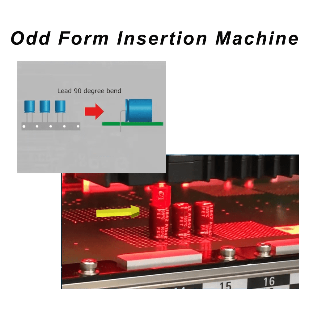
In the fast-paced world of electronic manufacturing, ensuring product quality is paramount. One way to achieve this is through various inspection methods, notably Automated Optical Inspection (AOI). By comparing AOI with other techniques, we can better appreciate its advantages and unique features.
Automatic Inspection vs. Manual Inspection
When it comes to inspection, the choice between automatic inspection and manual inspection can significantly impact efficiency and accuracy. Manual inspection often relies on human eyes to catch defects, which can lead to inconsistencies due to fatigue or oversight. In contrast, AOI inspection utilizes advanced machine vision systems that provide consistent results by analyzing each PCB with precision, ensuring that even the smallest solder paste inspection errors are detected.
Moreover, automated systems can process a higher volume of boards in less time compared to manual methods. This speed not only enhances productivity but also minimizes the risk of bottlenecks on production lines. Ultimately, while manual inspection has its place in certain scenarios, the reliability and efficiency of AOI make it a preferred choice for modern electronic manufacturing.
Cost Efficiency of Automated Systems
Cost efficiency is a crucial factor for any business looking to optimize operations in electronic manufacturing. Although the initial investment in automated optical inspection systems may seem steep compared to manual setups, the long-term savings are substantial. With reduced labor costs and fewer defects leading to rework or scrap materials, companies can see significant returns on their investment over time.
Additionally, AOI systems excel at identifying issues early in the production process through effective solder paste inspections and other vision inspection techniques. This early detection prevents costly downstream problems that could arise from undetected defects in PCBs. As such, businesses adopting automated systems often find themselves reaping financial benefits while maintaining high-quality standards.
Flexibility in Electronic Manufacturing
Flexibility is another area where AOI shines compared to traditional methods like manual inspections or older technologies. Modern machine vision systems used in optical inspections are designed with adaptability in mind; they can be configured for various types of PCBs and different production runs without extensive downtime or recalibration processes. This adaptability allows manufacturers to respond quickly to changing demands or product designs without sacrificing quality control.
Furthermore, as electronic products become more complex with intricate designs and smaller components, having an agile system for automated inspections becomes essential for maintaining competitive advantage in the market. The ability of AOI technology to evolve alongside these changes further solidifies its role as a cornerstone of effective quality assurance strategies within electronic manufacturing environments.
How Bensun Technology Implements AOI
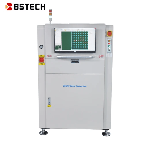
Bensun Technology is at the forefront of integrating Automated Optical Inspection (AOI) into electronic manufacturing processes. Their innovative solutions are designed to enhance quality control through precise optical inspection techniques, ensuring that every product meets the highest standards. With a focus on efficiency and reliability, Bensun’s AOI systems leverage cutting-edge machine vision systems to streamline production lines.
Overview of Bensun's AOI Solutions
Bensun offers a comprehensive range of AOI solutions tailored for various stages of PCB production. Their systems utilize advanced vision inspection techniques that can detect defects in real-time, significantly reducing the risk of faulty products reaching customers. From solder paste inspection to complete board inspections, Bensun’s automated inspection technology ensures thorough evaluation without compromising speed or accuracy.
Customizable AOI Systems for Clients
One standout feature of Bensun's offerings is the ability to customize their AOI systems according to client needs. This flexibility allows manufacturers to adjust parameters specific to their production requirements, whether it be for solder paste inspection or more complex board evaluations. By providing adaptable solutions, Bensun ensures that clients can achieve optimal results in electronic manufacturing while maintaining cost efficiency and effectiveness.
The Role of AOI in Bensun's Production Process
Incorporating AOI into its production process has been a game-changer for Bensun Technology. The automated inspection capabilities significantly enhance quality assurance by identifying defects early in the assembly line, which leads to reduced rework and waste. As a result, this integration not only improves yield rates but also positions Bensun as a leader in delivering high-quality electronic components efficiently.
Conclusion
In wrapping up our exploration of Automated Optical Inspection (AOI), it’s clear that this technology plays a pivotal role in enhancing quality control within electronic manufacturing. By leveraging machine vision systems and automated inspection techniques, manufacturers can significantly reduce defects and improve yield rates. The benefits of AOI inspection extend beyond mere cost savings; they also contribute to the overall efficiency and reliability of production lines.
Key Takeaways on AOI Benefits
The most compelling advantage of AOI is its ability to ensure high-quality standards in PCB production through precise optical inspection methods. Solder paste inspection is one area where AOI shines, detecting even the minutest discrepancies that manual inspections might overlook. Additionally, automated systems streamline the inspection process, allowing for faster turnaround times and greater flexibility in electronic manufacturing.
Future Trends in Optical Inspection
Looking ahead, the landscape of optical inspection is poised for exciting advancements driven by innovations in technology. Machine learning algorithms will likely enhance vision inspection techniques, enabling systems to learn from past inspections and improve their accuracy over time. Furthermore, as the demand for more complex electronics rises, we can anticipate a surge in sophisticated AOI solutions tailored to meet these evolving challenges.
How to Choose the Right AOI System
Selecting the right AOI system involves evaluating several key factors tailored to your specific needs within electronic manufacturing. Considerations should include the type of products being inspected—whether it’s PCB assemblies or solder paste applications—and how well various automated inspection solutions integrate with existing processes. Ultimately, investing time into understanding your requirements will lead you to an effective solution that maximizes both quality and efficiency in your production line.
