Introduction
In the fast-paced world of electronics, ensuring the quality and efficiency of printed circuit board (PCB) production is paramount. Enter automatic optical inspection (AOI), a game-changing technology that revolutionizes how we approach quality control in circuit board manufacturing. By utilizing advanced optical inspection techniques, manufacturers can detect defects early and streamline their processes, ultimately leading to superior products.
The Role of Automated Optical Inspection
Automated optical inspection plays a critical role in modern PCB production by providing a reliable means of identifying defects that could compromise functionality. This technology employs high-resolution cameras and sophisticated algorithms to analyze solder paste application and component placement on circuit boards with remarkable precision. As a result, AOI not only enhances the quality assurance process but also reduces the likelihood of costly rework or product failures.
Importance of PCB Quality and Efficiency
The importance of maintaining high-quality standards in PCB production cannot be overstated; even minor defects can lead to significant operational issues down the line. Efficient production processes are equally crucial, as they directly impact profitability and time-to-market for electronic devices. By implementing automatic optical inspection systems, manufacturers can ensure that their circuit boards meet rigorous quality benchmarks while optimizing overall efficiency in their production lines.
Overview of Optical Inspection Technology
Optical inspection technology encompasses various methods designed to enhance defect detection throughout the manufacturing process. From solder paste inspection to final assembly checks, these systems utilize light-based imaging techniques to scrutinize every aspect of a printed circuit board’s surface. As we delve deeper into this topic, we'll explore how these technologies work together to elevate PCB board production standards across the industry.
Understanding Automated Optical Inspection
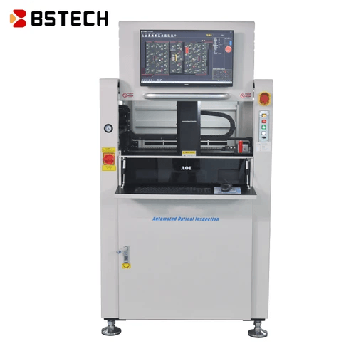
In the world of printed circuit board (PCB) production, ensuring quality is paramount, and this is where automatic optical inspection (AOI) comes into play. AOI serves as a crucial tool designed to detect defects in circuit boards during the manufacturing process. By employing sophisticated imaging technology, AOI systems help manufacturers maintain high standards of quality while enhancing efficiency.
Definition and Purpose of AOI
Automatic optical inspection is a non-contact method used to assess the quality of printed circuit boards by capturing images and analyzing them for defects. The primary purpose of AOI is to identify issues such as misaligned components, solder bridging, or insufficient solder paste application early in the production process. By catching these errors before they escalate into larger problems, AOI plays a vital role in ensuring that circuit board production remains reliable and efficient.
How AOI Works in PCB Production
In PCB production, automatic optical inspection operates by utilizing high-resolution cameras and advanced software algorithms to scan each board meticulously. These systems can compare captured images against predefined templates or specifications to identify discrepancies that may indicate defects. As a result, the integration of optical inspection technology allows for real-time monitoring during various stages of the manufacturing process, including solder paste inspection and final assembly checks.
Benefits for Circuit Board Quality Control
The benefits of incorporating AOI into circuit board quality control are numerous and impactful. Firstly, it significantly reduces the likelihood of defects reaching later stages in production or even worse—into consumer hands—thereby protecting brand reputation and customer satisfaction. Secondly, by streamlining processes such as solder paste inspection and automatic inspection routines, manufacturers can increase throughput while lowering costs associated with rework or scrap caused by faulty boards.
The Process of Optical Inspection
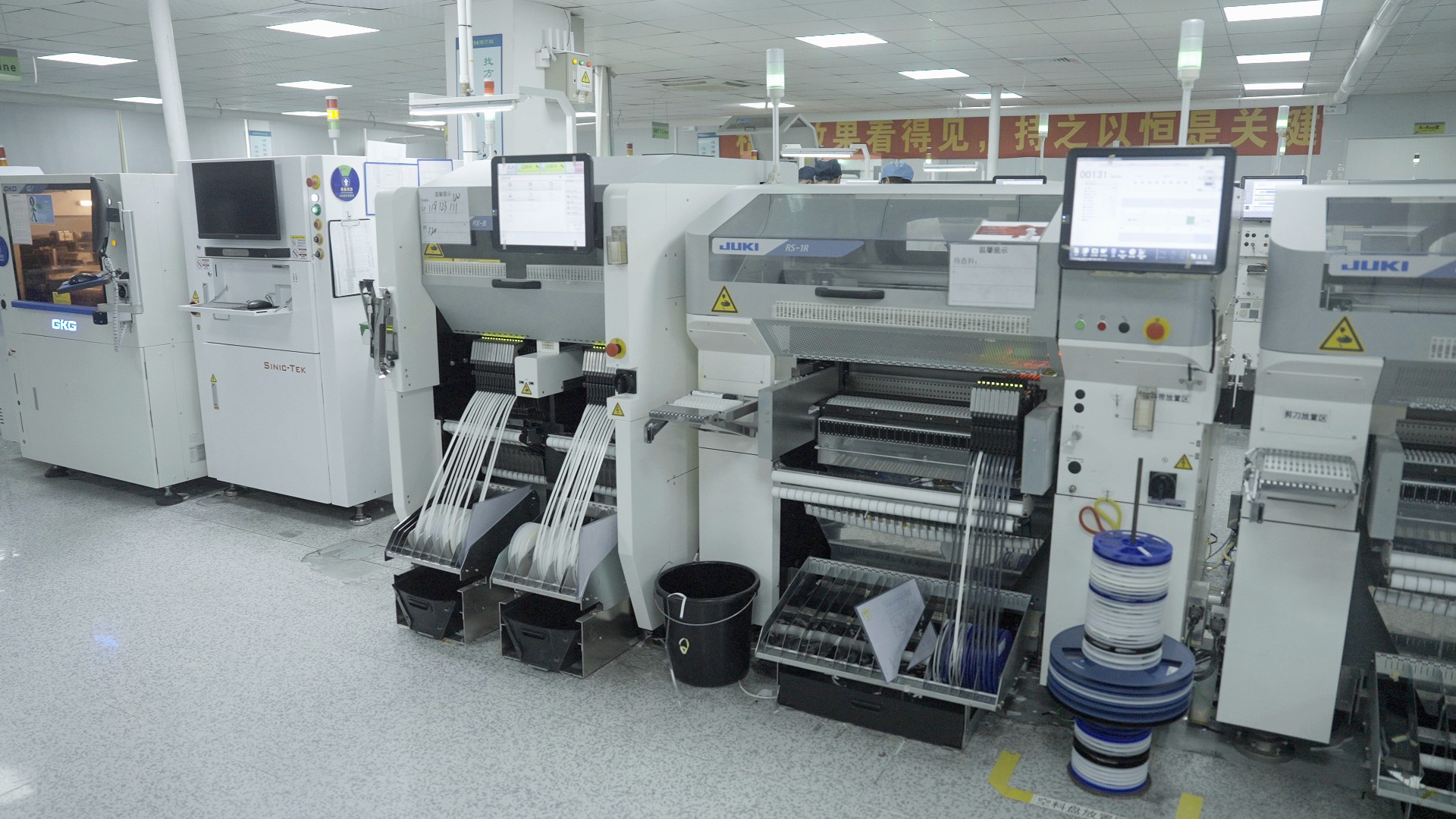
The process of optical inspection in printed circuit board production is a game-changer for manufacturers aiming to enhance quality and efficiency. By employing automatic optical inspection (AOI) systems, companies can detect defects early in the production line, significantly reducing the risk of faulty products reaching customers. This section delves into the essential steps involved in automatic inspection, the techniques used for solder paste inspection, and how to seamlessly integrate AOI into circuit board production processes.
Steps in Automatic Inspection
Automatic optical inspection involves a series of systematic steps designed to ensure that every circuit board meets stringent quality standards. Initially, the PCB is scanned using high-resolution cameras that capture detailed images of the board's surface and components. Next, these images are analyzed against predefined criteria to identify any discrepancies or defects, such as misplaced components or insufficient solder coverage, ensuring that only high-quality boards proceed further down the production line.
Once defects are detected through this rigorous automatic inspection process, operators receive immediate feedback on specific issues that need addressing. This real-time data allows manufacturers to make swift adjustments in their processes or rectify errors before they escalate into larger problems. Consequently, by incorporating these steps into their workflow, PCB manufacturers can maintain a high standard of quality control while minimizing waste and rework costs.
Solder Paste Inspection Techniques
Solder paste inspection is a critical component of ensuring reliable connections on printed circuit boards during assembly. Various techniques are employed to assess solder paste application quality before components are placed on the PCB. These methods include 2D and 3D imaging technologies; 2D inspections focus on measuring paste height and area coverage while 3D inspections provide depth information about solder deposits.
By utilizing advanced imaging systems within automatic optical inspection setups, manufacturers can quickly identify issues like insufficient or excessive solder paste application—both of which can lead to poor electrical connections or even complete failure of the circuit board. Regular implementation of these solder paste inspection techniques not only enhances product reliability but also serves as an early warning system for potential problems down the line in PCB board production processes.
Integrating AOI with Circuit Board Production
Integrating automatic optical inspection into circuit board production enhances overall efficiency while maintaining high-quality standards throughout manufacturing operations. The key lies in embedding AOI systems at strategic points along the production line—most notably after critical stages such as soldering and component placement—to catch errors immediately rather than waiting until later stages when corrections become costlier and more complex.
Moreover, seamless integration means that data collected during inspections can be fed back into manufacturing systems for continuous improvement efforts; this results in refined processes tailored specifically to minimize defect rates over time. As automated optical inspection becomes more sophisticated with advancements like AI-driven analytics, its integration within PCB manufacturing will only grow more vital—streamlining operations while ensuring top-notch product quality across all levels.
Enhancing Efficiency in PCB Board Production
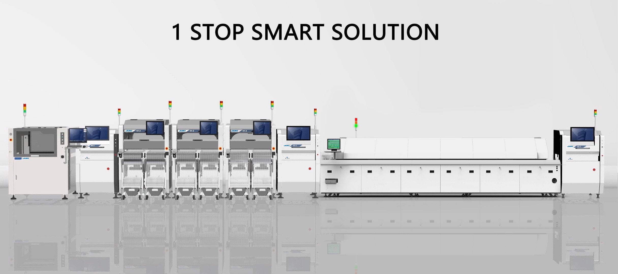
In the fast-paced world of printed circuit board production, efficiency is key to staying competitive. Automated optical inspection (AOI) plays a pivotal role in enhancing both quality and productivity within the circuit board manufacturing process. By integrating advanced optical inspection technology, manufacturers can significantly reduce defects and streamline their production lines.
Reducing Defects through AOI
One of the primary advantages of automatic optical inspection is its ability to drastically reduce defects in PCB board production. By employing high-resolution cameras and sophisticated algorithms, AOI systems can detect solder paste application issues, component misalignments, and other potential faults that could compromise circuit board integrity. This level of precision ensures that only boards meeting stringent quality standards make it through to the next stages of production.
Moreover, implementing optical inspection techniques early in the manufacturing process allows for immediate corrective actions, minimizing waste and rework costs. The result? A significant reduction in defective products reaching customers, which ultimately enhances brand reputation and customer satisfaction. In essence, AOI not only safeguards quality but also supports a more sustainable approach to circuit board production.
Streamlining the Production Line
Integrating automatic inspection into the PCB manufacturing workflow streamlines operations like never before. With real-time feedback provided by AOI systems, operators can quickly identify bottlenecks or inefficiencies within the production line. This responsiveness allows teams to adjust processes promptly—whether it’s recalibrating equipment or retraining staff on best practices for solder paste inspection.
Additionally, automated optical inspection reduces reliance on manual inspections that are often time-consuming and prone to human error. By automating these tasks, companies can allocate their skilled workforce to more strategic roles while maintaining high throughput levels in circuit board production. The cumulative effect is a leaner operation that not only saves time but also cuts costs associated with labor and materials.
Case Studies of Successful Implementations
Many manufacturers have successfully implemented automatic optical inspection systems with impressive results that speak volumes about their effectiveness in enhancing efficiency. For instance, one leading electronics manufacturer reported a 30% reduction in defect rates after integrating AOI into their printed circuit board production line—transforming both output quality and operational efficiency overnight.
Another case involved a mid-sized company specializing in high-mix low-volume assembly who adopted solder paste inspection technology as part of their AOI strategy. The outcome was remarkable; they saw an increase in first-pass yield from 85% to over 95%, allowing them to fulfill customer orders faster without compromising quality standards.
These success stories illustrate how embracing advanced optical inspection technologies not only mitigates risks associated with defects but also propels businesses toward greater profitability and growth within an increasingly competitive landscape.
Choosing the Right AOI Solution
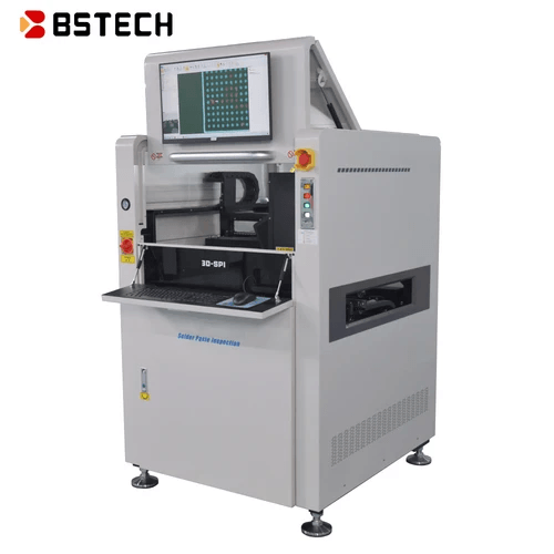
Selecting the right automatic optical inspection (AOI) system can feel like navigating a maze of options, but it’s crucial for optimizing your circuit board production. The right solution not only enhances quality control but also boosts efficiency and reduces costs in printed circuit board production. With various technologies available, understanding what fits your specific needs is key to successful implementation.
Factors to Consider in Selection
When choosing an AOI solution, several factors come into play that can significantly impact your circuit board production. First, consider the type of inspection required—whether you need solder paste inspection, component placement verification, or overall defect detection. Additionally, assess the speed and accuracy of the system; a high-speed automatic inspection machine may be necessary for larger volumes while ensuring precision in detecting minute defects.
Another vital aspect is integration capabilities with existing systems on your production line. The ideal AOI should seamlessly fit into your current workflow without causing bottlenecks or requiring extensive retraining for staff. Finally, don’t overlook after-sales support and software updates; a reliable vendor will provide ongoing assistance to keep your optical inspection system running smoothly.
Leading AOI Technologies in the Market
The market is buzzing with innovative AOI technologies that cater to diverse needs in PCB board production. Some leading players include systems that utilize advanced 3D imaging for enhanced depth perception during solder paste inspection, allowing for more accurate assessments of component placements and solder joints. Other notable technologies involve AI-driven algorithms that enable real-time learning from past inspections to improve future accuracy and efficiency.
Additionally, compact systems designed specifically for small-scale operations are gaining traction among startups looking to maintain high-quality standards without breaking the bank on larger equipment. These solutions often come equipped with user-friendly interfaces that simplify training processes and enhance overall usability on the production floor. Keeping an eye on these trends ensures you’re selecting a technology that's not just current but also future-proof.
How Bensun Technology Meets Your Needs
Bensun Technology stands out as a premier choice when it comes to automatic optical inspection solutions tailored for modern PCB manufacturing demands. With their cutting-edge systems designed specifically for efficient solder paste inspection and comprehensive automatic inspections throughout the entire circuit board production process, Bensun ensures no detail is overlooked in quality control efforts. Their robust integration capabilities mean you won’t face disruptions during transitions from older systems—an essential factor when considering long-term investments.
Moreover, Bensun’s commitment to customer support guarantees that you’ll have access to expert guidance as well as continuous software enhancements tailored to evolving industry standards and practices in printed circuit board production. By choosing Bensun Technology's AOI solutions, you're not just investing in equipment; you're securing a partner dedicated to elevating your operational efficiency while reducing costs associated with defects and rework.
Future Trends in Automated Optical Inspection
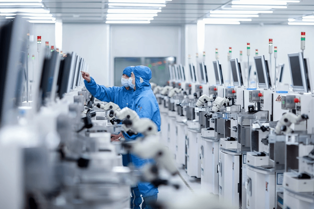
The landscape of automated optical inspection (AOI) is evolving rapidly, driven by technological advancements and the ever-increasing demand for high-quality circuit boards. Innovations on the horizon promise to enhance the capabilities of optical inspection systems, making them more efficient and effective in detecting defects during printed circuit board production. As manufacturers strive for perfection, these innovations will play a crucial role in shaping the future of PCB board production.
Innovations on the Horizon
One of the most exciting innovations in automatic optical inspection is the integration of advanced imaging technologies, such as 3D and multispectral imaging. These technologies allow for more detailed analysis of solder paste inspection and other critical areas on circuit boards, significantly improving defect detection rates. Additionally, new materials and components are being developed that can withstand higher temperatures and harsher environments, enhancing the reliability of AOI systems.
Another promising trend is the miniaturization of AOI equipment, which allows for easier integration into existing production lines without requiring extensive modifications. Smaller systems can provide real-time feedback during automatic inspection processes, enabling manufacturers to address defects immediately rather than at later stages. This agility not only improves efficiency but also reduces waste associated with faulty products.
Lastly, cloud-based solutions are emerging as game-changers for data management in PCB board production. By leveraging cloud technology, manufacturers can store vast amounts of inspection data securely while enabling remote access to analytics tools that help identify trends over time. This capability allows companies to continuously improve their quality control processes based on real insights gained from previous inspections.
The Role of AI in Optical Inspection
Artificial intelligence (AI) is set to revolutionize automated optical inspection by enhancing its capabilities beyond simple defect detection. AI algorithms can analyze complex patterns within solder paste inspection results that human operators might overlook, leading to more accurate assessments of circuit board quality. Moreover, machine learning models can adapt over time as they process more data from various production runs, continuously refining their ability to detect anomalies.
Incorporating AI into AOI systems also means improved predictive maintenance capabilities; machines equipped with intelligent software can forecast when components are likely to fail or require servicing based on historical performance data from previous inspections. This proactive approach minimizes downtime during printed circuit board production and increases overall efficiency across manufacturing operations. With AI handling routine tasks such as image recognition and defect classification, human operators can focus on higher-level decision-making processes.
Furthermore, AI-powered systems enable better integration between different stages of PCB board production by facilitating seamless communication between machines involved in various processes like assembly or testing. This interconnectedness ensures a smoother workflow where issues detected during automatic inspection are immediately relayed back to relevant teams for swift resolution—ultimately leading to enhanced product quality.
Predictions for PCB Production Advances
Looking ahead at future trends in automated optical inspection reveals several exciting predictions about how technology will shape PCB board production practices over the next decade. One major prediction is that we will see an increasing reliance on automation throughout every aspect of manufacturing—from sourcing raw materials through final assembly—resulting in faster turnaround times without compromising quality standards due largely due improvements within AOI technologies themselves.
We may also witness greater collaboration between manufacturers across different sectors as they share best practices related specifically towards implementing effective automatic optical inspections tailored toward their unique needs while benefiting collectively from shared knowledge gained through experiences encountered along their respective journeys towards achieving optimal results within solder paste inspections among other key areas critical towards ensuring high-quality outputs consistently delivered across diverse applications utilizing printed circuit boards produced efficiently using advanced methodologies available today!
Lastly—and perhaps most intriguingly—the potential emergence of fully autonomous factories capable not only performing all necessary tasks involved throughout each stage required producing high-quality PCBs but also intelligently managing workflows autonomously based upon real-time insights gathered via sophisticated analytics platforms monitoring every step taken along this intricate journey promises an exciting new era where human intervention becomes increasingly optional rather than mandatory!
Conclusion
In the world of circuit board production, the integration of automatic optical inspection (AOI) technology has proven to be a game changer. Not only does it enhance the quality of printed circuit board production, but it also drastically reduces the likelihood of defects during manufacturing. As we've explored, understanding and implementing effective optical inspection techniques is essential for any PCB manufacturer aiming for excellence.
Key Takeaways on AOI Benefits
Automatic optical inspection serves as a critical checkpoint in the circuit board production process, ensuring that each component meets stringent quality standards. The benefits are clear: improved defect detection rates lead to higher reliability in end products and greater customer satisfaction. Moreover, by incorporating solder paste inspection into their workflows, manufacturers can catch issues early on, saving both time and resources.
Enhancing Quality and Reducing Costs
With AOI systems in place, manufacturers can significantly enhance product quality while simultaneously reducing costs associated with rework and waste. The precision offered by automatic inspection minimizes human error and delivers consistent results that manual processes simply cannot match. Consequently, PCB board production becomes more efficient, allowing companies to allocate resources more effectively and maintain competitive pricing.
The Future of Circuit Board Manufacturing
Looking ahead, the future of circuit board manufacturing will undoubtedly be shaped by advancements in automatic optical inspection technology. Innovations such as AI-driven analysis will further refine defect detection capabilities and streamline workflows in printed circuit board production environments. As these technologies evolve, we can expect even greater efficiencies and improvements in product quality across the industry.
