Introduction

In the world of electronics, circuit board inspection is a critical process that ensures the reliability and functionality of electronic devices. From smartphones to complex industrial machinery, printed circuit assembly (PCA) forms the backbone of modern technology. Understanding the nuances of circuit card assembly and the various techniques employed for inspection can significantly impact product quality and performance.
Understanding Circuit Board Inspection
Circuit board inspection encompasses a range of techniques aimed at identifying defects in printed circuit boards (PCBs). This process is essential for ensuring that every component on a PCB functions correctly within its designated parameters. Whether it’s visual checks or advanced optical inspection methods, each step plays a vital role in maintaining high standards in printed board assembly.
Importance of PCB Inspection Techniques
The importance of PCB inspection techniques cannot be overstated; they directly influence product reliability and customer satisfaction. By implementing rigorous inspection protocols, manufacturers can detect issues early in the production process, preventing costly recalls or failures down the line. Moreover, effective circuit board inspection contributes to streamlined production workflows, enhancing efficiency while minimizing waste.
Overview of Equipment Used
A variety of equipment is utilized in circuit board inspection to ensure thorough evaluation and testing. From automated optical systems to X-ray machines, these tools help identify even the smallest defects that could compromise a PCB's integrity. Understanding this equipment’s role not only aids in improving printed circuit assy quality but also enhances overall manufacturing processes.
Types of Circuit Board Inspection

When it comes to ensuring the integrity and functionality of circuit board assemblies, various inspection methods are employed. Each technique offers unique advantages, catering to different aspects of printed circuit assembly (PCA) and printed board assembly (PBA). Understanding these types helps manufacturers choose the most effective approach for their specific needs.
Visual Inspection Methods
Visual inspection methods remain a staple in circuit board inspection due to their simplicity and effectiveness. This technique involves a careful examination of the circuit card assembly by trained personnel who look for visible defects such as soldering issues, component misalignment, or other anomalies. While this method relies heavily on human judgment, it can be enhanced with magnifying tools or microscopes to improve detection rates.
One notable advantage of visual inspection is its cost-effectiveness; it requires minimal equipment compared to more advanced techniques. However, it may not catch all defects, especially those hidden from view on multi-layered PCBs where intricate designs are involved. Thus, while visual inspections are important in the overall quality assurance process, they often need to be supplemented with more sophisticated methods for comprehensive verification.
Automated Optical Inspection
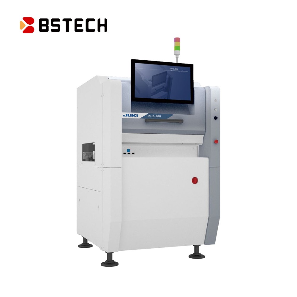
Automated Optical Inspection (AOI) has revolutionized circuit board inspection by integrating technology into quality control processes. AOI systems utilize high-resolution cameras and sophisticated software algorithms to scan the surface of printed circuit assemblies at high speed. This method allows for real-time defect detection and significantly reduces human error associated with manual inspections.
The benefits of AOI extend beyond just speed; they also include consistency in results and the ability to handle complex PCB designs that might overwhelm human inspectors. By analyzing images captured during the inspection process, AOI can identify issues such as missing components or insufficient solder joints with remarkable accuracy. As a result, many manufacturers have adopted automated optical inspection as a critical component in their PCB assembly workflow.
X-Ray Inspection Techniques
X-ray inspection techniques provide an invaluable tool for evaluating internal structures within multi-layered circuit boards that are otherwise invisible during standard inspections. This non-destructive testing method allows engineers to assess solder joint integrity and verify layer alignment within printed circuit assemblies without damaging them. Particularly useful for detecting hidden defects like voids in solder joints or misaligned components, X-ray technology is essential for high-reliability applications.
While X-ray systems tend to be more expensive than other forms of circuit board inspection due to their advanced technology requirements, they offer unparalleled insights into complex assemblies like those found in medical devices or aerospace applications where failure is not an option. The ability to visualize internal structures ensures that manufacturers maintain high standards throughout their production processes. In a world increasingly reliant on sophisticated electronic devices, X-ray techniques represent a crucial advancement in ensuring quality within printed board assemblies.
Essential PCB Inspection Equipment

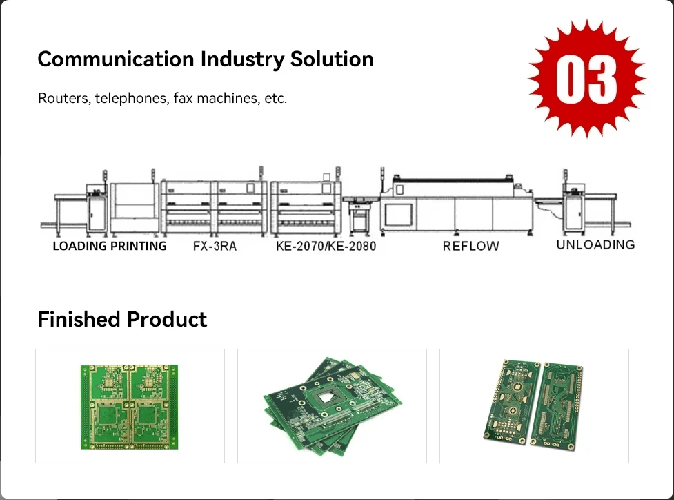
In the realm of circuit board inspection, having the right equipment is crucial for ensuring high-quality printed circuit assembly (PCA). This section will delve into two essential tools: JUKI pick and place machines and reflow ovens. These pieces of equipment play a pivotal role in enhancing the efficiency and accuracy of circuit card assembly processes.
JUKI Pick and Place Machines
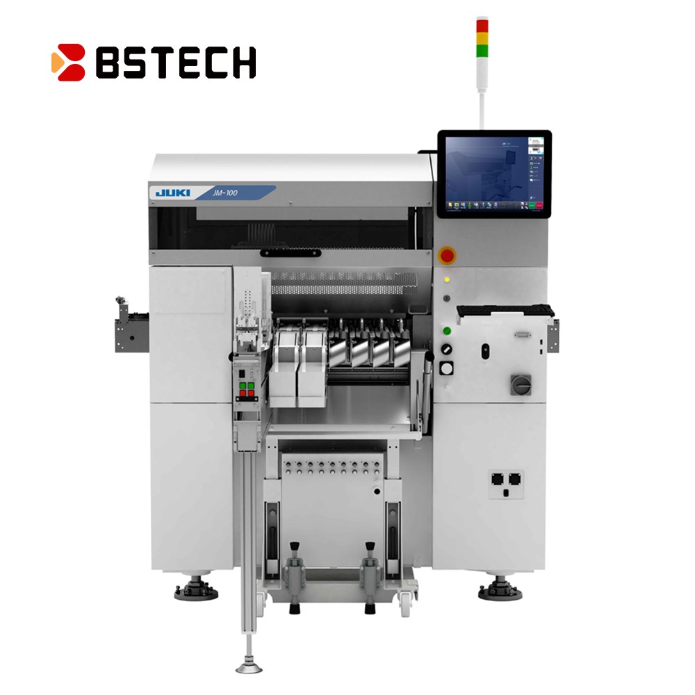
JUKI pick and place machines are renowned for their precision in placing components on printed circuit boards (PCBs). These machines automate the process, significantly reducing human error, which is vital in circuit board inspection. With advanced features like vision systems, they ensure that every component is correctly positioned, laying a solid foundation for effective optical inspection later in the assembly line.
Moreover, JUKI machines are designed to handle various component types and sizes, making them versatile for different printed board assembly (PBA) requirements. Their speed allows for higher production rates without compromising quality—an essential factor when scaling up production volumes. By integrating JUKI pick and place technology into your workflow, you not only streamline your operations but also enhance overall reliability in your PCB assembly board processes.
Reflow Ovens and Their Role
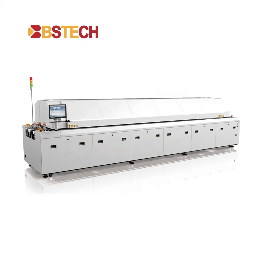
Reflow ovens play an indispensable role in the printed circuit assembly process by ensuring that solder joints are properly formed during manufacturing. After components have been placed on the PCB by machines like JUKI, these ovens heat up to melt solder paste applied earlier during assembly. This process creates strong electrical connections critical for optimal performance during circuit board inspection.
The ability of reflow ovens to provide uniform heating helps avoid common issues such as cold solder joints or bridging—both detrimental to effective circuit card assembly. Additionally, modern reflow ovens come equipped with sophisticated temperature profiling capabilities that allow manufacturers to optimize their processes further. By investing in high-quality reflow technology, companies can significantly improve their yield rates while ensuring that every printed circuit assy meets stringent quality standards.
Techniques for Effective Circuit Card Assembly

When it comes to circuit card assembly, ensuring quality is paramount. A well-executed printed circuit assembly (PCA) not only enhances performance but also reduces the risk of failures in the field. To achieve this, several techniques are employed during the inspection and assembly phases, focusing on critical areas such as solder joints and layer alignment.
Solder Joint Inspection
Solder joint inspection is a crucial step in circuit board inspection that ensures reliable electrical connections. Inspectors look for defects such as cold solder joints, bridging, or insufficient wetting that could compromise the integrity of the printed board assembly (PBA). By utilizing advanced optical inspection methods and automated systems, manufacturers can quickly identify and rectify these issues before they escalate into costly problems.
Effective solder joint inspection often employs a combination of visual checks and automated optical inspection (AOI) systems. These systems use high-resolution cameras to capture detailed images of each joint, allowing for precise measurements and assessments. Regular inspections not only improve the quality of printed circuit assemblies but also enhance overall production efficiency by minimizing rework.
Layer Alignment Checks
Layer alignment checks are essential in ensuring that all components on a circuit board are correctly positioned relative to one another. Misalignment can lead to performance issues or even complete failure of electronic devices, making this step vital in the PCB assembly process. By employing sophisticated optical inspection techniques, manufacturers can detect misalignments at various stages of production.
During layer alignment checks, inspectors focus on both horizontal and vertical alignments within multilayer PCBs. Advanced imaging technology allows for real-time monitoring and adjustments during assembly, significantly reducing errors associated with manual inspections. This proactive approach not only enhances product reliability but also streamlines workflow in printed circuit assy processes.
Comprehensive Testing Protocols
Comprehensive testing protocols are integral to ensuring that every aspect of the circuit card assembly meets stringent quality standards. These protocols typically include functional testing, thermal cycling tests, and electrical continuity checks to verify that all components operate as intended under various conditions. Implementing rigorous testing measures helps identify potential failures early on in the production cycle.
Incorporating comprehensive testing into the PCB inspection process aids in maintaining high-quality standards throughout production runs. Additionally, these protocols serve as a safeguard against defects that could lead to significant operational issues down the line. Ultimately, thorough testing not only boosts confidence in product reliability but also reinforces customer trust in your brand's commitment to excellence.
Advanced Optical Inspection Techniques

In the realm of circuit board inspection, advanced optical techniques play a pivotal role in ensuring the reliability and performance of printed circuit assemblies (PCAs). These methods enhance the accuracy and efficiency of inspections, addressing the complexities that arise during circuit card assembly. By leveraging cutting-edge technology, manufacturers can significantly reduce defects and improve overall product quality.
3D Optical Inspection Systems
3D optical inspection systems are revolutionizing how we approach circuit board inspection. Unlike traditional 2D methods, these systems provide a comprehensive three-dimensional view of the printed board assembly, allowing for precise measurements and assessments of component placement and solder joints. This depth perception is crucial for identifying potential issues that might be missed with less sophisticated inspection techniques.
The integration of 3D optical systems into the PCB assembly process not only streamlines inspections but also enhances quality assurance protocols. By capturing detailed topography data, manufacturers can detect discrepancies in layer alignment and component height that could lead to failures down the line. Ultimately, this technology elevates the standards for printed circuit assy by ensuring every detail is meticulously examined.
Use of Machine Vision
Machine vision technology has become indispensable in modern circuit board inspection processes. By utilizing sophisticated algorithms and image processing capabilities, machine vision systems can quickly analyze large volumes of data to identify defects or anomalies in real-time during printed circuit assembly operations. This automation reduces human error and speeds up production without compromising on quality.
Moreover, machine vision systems are capable of adapting to various types of PCBs, making them versatile tools for manufacturers dealing with diverse product lines. From detecting misaligned components to evaluating solder joint integrity, these systems enhance the overall efficiency of inspections within the PCB assembly workflow. As a result, businesses can ensure their products meet stringent quality standards while maintaining competitive timelines.
Benefits of High-Resolution Cameras
High-resolution cameras are a game-changer in optical inspection for printed circuit assemblies (PCAs). These cameras capture intricate details that are essential for thorough circuit board inspection; they enable inspectors to zoom in on critical areas without losing image clarity or detail fidelity. The ability to discern fine features ensures that even subtle defects do not go unnoticed during assessments.
Additionally, high-resolution imaging contributes significantly to improving defect detection rates across various stages of circuit card assembly. With clearer visuals at their disposal, inspectors can make informed decisions swiftly—whether it’s approving a batch or flagging concerns for further analysis. In an industry where precision is paramount, investing in high-resolution camera technology pays dividends by enhancing both product reliability and customer satisfaction.
Best Practices in Printed Circuit Assembly

In the world of printed circuit assembly, ensuring quality and reliability is paramount. Adopting best practices not only enhances the integrity of circuit card assembly but also minimizes costly errors down the line. This section delves into three key areas: regular maintenance of inspection equipment, training staff on inspection protocols, and integrating inspection into the production workflow.
Regular Maintenance of Inspection Equipment
Regular maintenance of inspection equipment is crucial for effective circuit board inspection. Just like a well-tuned engine, properly maintained machines yield better performance and more accurate results during optical inspections. Schedule routine checks for your PCB assembly board tools to ensure they function optimally, reducing downtime and enhancing the overall efficiency of printed board assembly processes.
Moreover, keeping your equipment clean and calibrated not only extends its lifespan but also ensures that every component is scrutinized to meet stringent quality standards. Any misalignment or malfunction can lead to significant issues in circuit card assembly, so proactive maintenance should be a non-negotiable part of your operational strategy. Remember, an ounce of prevention is worth a pound of cure when it comes to maintaining quality in printed circuit assy.
Training Staff on Inspection Protocols
Investing time in training staff on inspection protocols can dramatically improve the effectiveness of your circuit board inspection processes. Well-trained personnel are better equipped to identify potential issues during visual inspections or automated optical inspections, leading to higher-quality outcomes in printed circuit assembly. Regular workshops and hands-on training sessions keep everyone updated on best practices and new technologies related to PCB assembly.
Furthermore, fostering a culture that emphasizes continuous learning helps create an environment where employees feel empowered to contribute ideas for improvement in circuit card assembly techniques. Encourage team members to share their experiences with different types of inspections; this knowledge exchange can lead to innovative solutions that enhance overall efficiency. After all, an informed workforce is one that can adapt quickly to evolving industry standards.
Integrating Inspection into Production Workflow
Integrating inspection seamlessly into the production workflow is vital for achieving optimal results in printed board assembly. By embedding circuit board inspection at various stages—rather than treating it as a final checkpoint—you create multiple opportunities for quality assurance throughout the process. This proactive approach allows teams to catch potential defects early on, making it easier and less costly to address issues before they escalate.
Additionally, using real-time monitoring systems can provide instant feedback during production cycles, allowing operators to make immediate adjustments if necessary—this agility is essential for maintaining high standards in PCB assembly operations. Collaboration between departments ensures that everyone understands their role concerning quality control measures related to optical inspections and other testing methods employed throughout production lines. Ultimately, integrating these practices will enhance product reliability while boosting overall efficiency across all aspects of printed circuit assy.
Conclusion

In the ever-evolving world of electronics, circuit board inspection stands as a critical component in ensuring product reliability and performance. The techniques and equipment used in printed circuit assembly (PCA) are vital for maintaining quality throughout the manufacturing process. By implementing effective inspection methods, manufacturers can significantly reduce defects and enhance overall efficiency.
Key Takeaways on PCB Inspection
PCB inspection is essential to guarantee that each circuit card assembly meets stringent quality standards. Utilizing a combination of visual inspections, automated optical inspection, and advanced techniques like X-ray inspection ensures that potential issues are caught early in the production line. Moreover, regular maintenance of inspection equipment and staff training on protocols can lead to improved outcomes in printed board assembly.
Future Trends in Circuit Board Technologies
The future of circuit board technologies points toward increasingly sophisticated optical inspection systems that leverage artificial intelligence and machine learning for enhanced accuracy. As the demand for miniaturization grows, innovations will focus on improving the precision of inspections at smaller scales while maintaining high throughput rates. Additionally, advancements in materials used for PCBs may necessitate new inspection methodologies to adapt to evolving manufacturing processes.
Leading Companies in PCB Inspection Equipment
Several industry leaders dominate the field of PCB inspection equipment, providing cutting-edge solutions for manufacturers worldwide. Companies like JUKI offer innovative pick-and-place machines designed to streamline circuit card assembly processes while ensuring high-quality standards are met during printed circuit assembly tasks. Other notable players include companies specializing in optical inspection systems that continue to push the boundaries of technology in the realm of printed circuit assy.
