Introduction
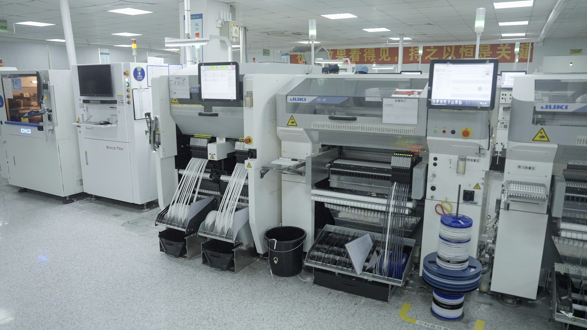
In the ever-evolving world of electronics, understanding how PCBs are made is crucial for both manufacturers and designers alike. Printed circuit board assembly (PCBA) serves as the backbone of modern electronic devices, connecting components in a compact and efficient manner. As technology advances, so do the techniques involved in circuit card assembly, making quality assurance more important than ever.
The Basics of PCB Manufacturing
At its core, PCB manufacturing involves creating a base that supports and connects electronic components through conductive pathways. The process typically starts with designing a printed circuit board layout, which is then transformed into a physical product through various fabrication techniques. Understanding the basics of PCB and assembly processes lays the groundwork for appreciating the complexities involved in printed circuit board assembly.
Evolution of PCB Assembly Technology
The journey from traditional methods to advanced technologies in printed circuit assembly has been nothing short of revolutionary. Initially dominated by manual labor and rudimentary tools, PCB assembly has seen significant advancements with the introduction of automated systems and sophisticated machinery. This evolution not only enhances efficiency but also ensures higher precision in circuit board assembly, ultimately leading to better-performing electronic products.
Importance of Quality in PCB Assembly
Quality control is paramount in PCB board assembly; any flaws can lead to catastrophic failures in electronic devices. Ensuring high-quality standards during each step—from design to fabrication—directly impacts the reliability and longevity of the final product. Therefore, focusing on quality throughout the entire printed circuit board assembly process is essential for manufacturers aiming to deliver exceptional electronics that meet consumer expectations.
Understanding PCB Design
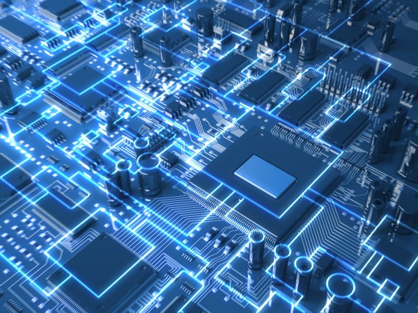
Designing a printed circuit board (PCB) is like crafting the blueprint for a complex machine. It involves intricate planning, creativity, and technical know-how to ensure that the final product functions as intended. In this section, we will explore key components of PCB design, the software tools that aid in layout creation, and the importance of prototyping in refining designs before moving to production.
Key Components of PCB Design
At its core, PCB design consists of several essential components that dictate how the circuit board assembly will function. These include traces (the paths that connect different components), pads (the areas where components are soldered), and vias (the small holes that allow connections between different layers). Understanding how these elements interact is crucial for anyone asking how are PCBs made and looking to ensure effective printed circuit assembly.
Moreover, component placement is critical; it influences both performance and manufacturability. A well-designed layout minimizes signal interference while optimizing space on the board—crucial for compact electronic devices. As such, mastering these key components is foundational for successful circuit card assembly.
Software Tools for PCB Layout
In today's digital age, sophisticated software tools have revolutionized how PCBs are designed. Programs like Altium Designer, Eagle, and KiCAD provide designers with powerful features to create precise layouts efficiently. These tools not only streamline the process but also help in simulating electrical performance before any physical prototype is made.
Using these software solutions allows designers to visualize their work in 3D—making it easier to spot potential issues early on in the design phase. This capability significantly reduces errors during printed circuit board assembly later on, saving both time and resources. Thus, leveraging advanced software tools is vital for anyone involved in PCB and assembly processes.
The Role of Prototyping in Design
Prototyping serves as a crucial step in PCB design by allowing engineers to test their theories before finalizing production plans. By creating a physical model of their design—often referred to as a proof of concept—designers can identify flaws or inefficiencies that might not be apparent on screen alone. This iterative process ensures high-quality outcomes when moving toward full-scale printed circuit board assembly.
Additionally, prototyping helps establish whether all components fit correctly within the designated space while maintaining functionality under real-world conditions. It’s an invaluable part of ensuring successful circuit board assembly by minimizing risks associated with manufacturing defects or functional failures down the line. Ultimately, investing time into prototyping pays off by enhancing reliability and performance in final products.
The PCB Fabrication Process
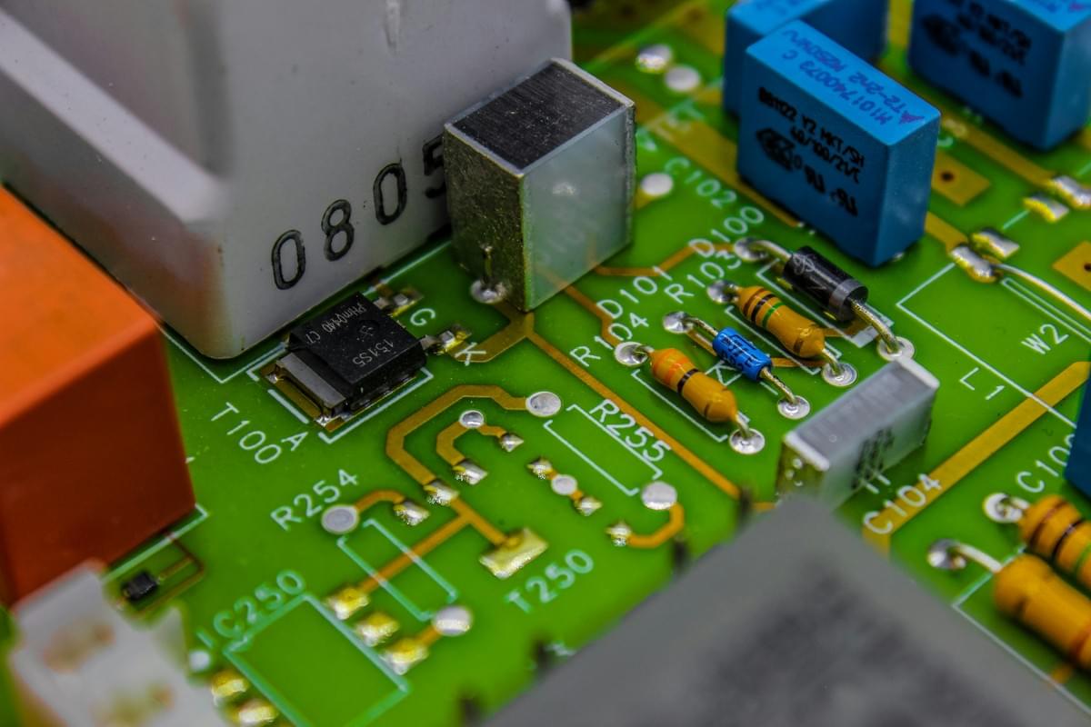
The PCB fabrication process is a critical phase in printed circuit board assembly, transforming raw materials into functional circuit boards ready for assembly. Understanding how PCBs are made involves a blend of science and artistry, where precision meets creativity. Each step in this intricate process plays a vital role in ensuring the reliability and performance of the final product.
Materials Used in PCB Manufacturing
The journey of how PCBs are made begins with selecting the right materials, which are fundamental to the quality and functionality of the circuit board assembly. Commonly used materials include fiberglass epoxy resin for the substrate, copper foil for conductive pathways, and solder mask to protect these pathways from environmental damage. Additionally, various types of laminates are chosen based on thermal and electrical properties to ensure optimal performance during operation.
Choosing high-quality materials is essential because they directly impact not only the durability but also the efficiency of printed circuit assembly. For instance, using superior copper foil can enhance conductivity, while high-grade substrates can improve heat dissipation. Ultimately, these material choices influence both production costs and long-term reliability in circuit board assembly.
Step-by-Step Fabrication Techniques
Understanding how PCBs are made involves delving into several key fabrication techniques that transform raw materials into finished boards ready for use. The process typically begins with designing a layout using CAD software before transferring this design onto a laminate through photolithography techniques. This is followed by etching away excess copper to create traces that form electrical connections on the PCB.
Next comes drilling holes for components and vias—small plated holes that allow connections between different layers of multilayer boards—before applying solder mask to protect against oxidation and short circuits during operation. Afterward, surface finish treatments such as ENIG or HASL are applied to ensure reliable soldering during printed circuit board assembly. Each step must be executed with care; any errors can lead to defects that compromise the entire circuit card assembly.
Importance of Fabrication Quality
Quality control during fabrication is paramount because it significantly affects not just how PCBs are made but also their overall performance in real-world applications. High fabrication quality ensures that each printed circuit board meets strict electrical specifications while minimizing defects such as shorts or open circuits that could lead to failure later on in production or use phases.
Moreover, rigorous testing protocols throughout the fabrication process help identify potential issues early on, reducing costly rework down the line during printed circuit assembly stages. In an industry where precision matters immensely, investing time and resources into maintaining high standards during fabrication pays off by enhancing reliability in final products—after all, nobody wants their gadgets malfunctioning due to poor-quality PCBs!
Overview of PCB Assembly Equipment

Types of Equipment for PCB Assembly
In the realm of printed circuit assembly, several types of equipment play crucial roles in ensuring efficiency and accuracy. From solder paste printers to pick-and-place machines, each piece of machinery is designed with specific tasks in mind that contribute to seamless circuit board assembly. Additionally, reflow ovens and inspection systems are vital for ensuring that each PCB board assembly meets stringent quality standards.
Solder paste printers apply a precise amount of solder paste onto pads on the PCB before components are placed. Pick-and-place machines then accurately position components onto these pads, while reflow ovens heat up the boards to create strong electrical connections through soldering. Finally, automated optical inspection (AOI) systems check for defects in real-time during production, ensuring that any issues are caught early on in the process.
Leading Brands and Their Innovations
The world of PCB assembly is filled with renowned brands pushing boundaries through innovation. Companies like ASM Assembly Systems and Panasonic have developed cutting-edge technology that enhances speed and precision in circuit card assembly processes. Their machines often incorporate advanced features such as artificial intelligence for better defect detection or modular designs that allow manufacturers to scale operations easily.
Another noteworthy player is Juki Automation Systems, known for its high-speed pick-and-place machines that can handle a variety of component sizes with ease. These brands continuously invest in research and development to stay ahead in an ever-evolving industry where efficiency directly impacts profitability. By choosing equipment from these leading brands, businesses can enhance their printed circuit board assembly capabilities significantly.
Comparing SMT vs. Through-Hole Technology
When discussing how are PCBs made, one must consider two primary methods: Surface Mount Technology (SMT) and Through-Hole Technology (THT). While both techniques serve similar purposes—mounting electronic components onto PCBs—they differ significantly in their application methods and suitability for various projects.
SMT involves placing components directly onto the surface of a PCB using automated machinery; this method allows for compact designs with higher component density—ideal for modern electronics where space is at a premium. Conversely, THT requires drilling holes into the PCB where leads from components are inserted; this technique is often favored for larger components or applications requiring robust connections due to its mechanical strength.
Ultimately, choosing between SMT and THT depends on factors such as design complexity, component size requirements, and production volume needs—all crucial considerations when planning your printed circuit board assembly workflow.
The PCB Assembly Process Explained
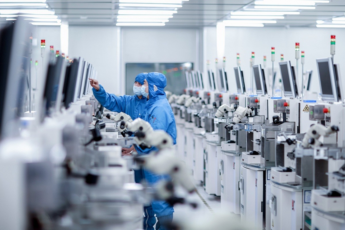
When it comes to creating electronic devices, understanding how printed circuit boards (PCBs) are assembled is crucial. The PCB assembly process transforms a design into a functional circuit card assembly that can power everything from smartphones to complex industrial machinery. This section will delve into the steps involved in printed circuit board assembly, the techniques that ensure high-quality soldering, and how visual inspection plays a vital role in enhancing overall quality.
Steps in Circuit Card Assembly
The journey of circuit board assembly starts with preparing the bare PCB, which is the foundation for all components. First, components are placed on the board using either manual or automated methods, often employing pick-and-place machines for precision and speed. Once components are positioned correctly, the next step involves soldering them to the PCB—this can be done through wave soldering or reflow soldering techniques depending on whether it's surface-mount technology (SMT) or through-hole technology being utilized.
After soldering, additional processes such as applying protective coatings and testing follow to ensure that each printed circuit board assembly meets quality standards. Functional testing checks for electrical connections and component integrity while visual inspections help catch any physical defects before products go out into the world. Ultimately, this meticulous process ensures that every PCB board assembly is ready for reliable performance in its intended application.
Importance of Soldering Techniques
Soldering is arguably one of the most critical aspects of PCB and assembly; it’s where electrical connections come to life! The choice of soldering technique—whether wave soldering for through-hole components or reflow soldering for SMT—can significantly impact both performance and reliability of the final product. High-quality solder joints ensure minimal risk of failures due to poor connections while enhancing durability against environmental stressors like heat and vibration.
Moreover, skilled technicians employ various methods during this phase to achieve optimal results—such as controlling temperature profiles during reflow processes or ensuring proper flux application beforehand. Understanding how PCBs are made with attention to detail during these stages can lead to superior printed circuit board assemblies that stand up against time and usage demands. In essence, mastering these techniques translates directly into better product outcomes.
How Visual Inspection Enhances Quality
Visual inspection serves as a final checkpoint in ensuring quality throughout the entire printed circuit assembly process. Before any product leaves production facilities, trained inspectors meticulously examine each circuit card assembly for defects such as misaligned components or inadequate solder joints—a crucial step since many issues may not be caught by automated testing alone! This human touch helps maintain high standards across all PCBs produced.
Additionally, advancements in technology have introduced automated optical inspection (AOI) systems that complement traditional visual checks by quickly scanning boards for defects at high speeds without compromising accuracy. By integrating both approaches into their quality assurance protocols, manufacturers reinforce their commitment to delivering top-notch PCB board assemblies that customers can trust wholeheartedly. Ultimately, effective visual inspection not only enhances product reliability but also boosts customer satisfaction—a win-win situation!
Choosing the Right PCB Assembly Partner

When it comes to printed circuit board assembly, selecting the right partner can make all the difference in your project's success. A reliable PCB assembly partner not only ensures high-quality circuit card assembly but also aligns with your specific needs and production goals. With a multitude of options available, it's crucial to assess various factors that can impact your overall experience and product quality.
Factors to Consider in a Partner
First and foremost, consider the partner's expertise in PCB manufacturing and assembly processes. Understanding how PCBs are made is essential; thus, look for companies that have a proven track record in printed circuit assembly and circuit board assembly technologies. Additionally, evaluate their capacity for scalability—can they handle large orders without compromising quality?
Another critical aspect is their commitment to quality assurance practices. Quality control measures should be robust throughout the PCB fabrication process, from initial design to final inspection of printed circuit board assembly. Finally, communication is key; ensure that your partner maintains transparency regarding timelines, challenges, and progress updates throughout your project.
Benefits of Working with Bensun Technology
Bensun Technology stands out as an exceptional choice for PCB assembly due to its combination of experience and innovation in the field. Their extensive knowledge of how PCBs are made allows them to provide tailored solutions that meet diverse client needs while maintaining high standards in printed circuit board assembly quality. Moreover, Bensun employs cutting-edge technology which enhances efficiency during the circuit card assembly process.
Working with Bensun also means you benefit from their strong customer support system; they prioritize building lasting relationships with clients by ensuring open lines of communication throughout every stage of production. This level of dedication not only fosters trust but also leads to better outcomes for both parties involved in the PCB and assembly process.
Understanding Pricing Models in PCB Assembly
Pricing models for PCB board assembly can vary widely depending on several factors including complexity, volume, and materials used. It's essential to understand how these elements influence costs so you can make informed decisions when comparing potential partners for your project. Some companies offer fixed pricing models based on standardized services while others may provide custom quotes based on specific requirements related to printed circuit board assemblies.
Additionally, keep an eye out for hidden costs such as expedited shipping fees or charges associated with revisions during prototyping stages—these can sneak up on you! By being proactive about understanding pricing structures upfront, you’ll ensure that your budget aligns seamlessly with the expectations set forth during initial discussions about how are PCBs made.
Conclusion
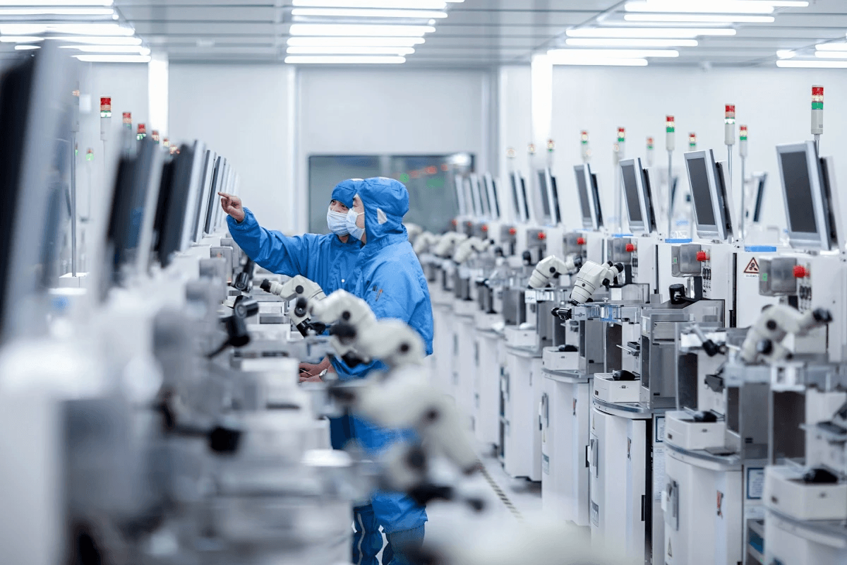
In conclusion, the landscape of PCB assembly is continually evolving, driven by technological advancements and market demands. Understanding how PCBs are made is essential for anyone involved in electronics, as it lays the foundation for effective circuit board assembly processes. As we look to the future, several trends will shape printed circuit board assembly, enhancing both quality and efficiency.
Future Trends in PCB Assembly
The future of PCB assembly is bright and filled with innovation. One major trend is the increasing miniaturization of components, which allows for more compact designs without sacrificing performance in circuit card assembly. Additionally, sustainability practices are becoming paramount; manufacturers are seeking eco-friendly materials and processes that reduce waste while maintaining high standards in printed circuit assembly.
Enhancing Efficiency in PCB Manufacturing
To enhance efficiency in PCB manufacturing, companies are adopting lean manufacturing principles that streamline operations and minimize waste. Techniques such as just-in-time inventory management ensure that materials needed for printed circuit board assembly are available when required without excess stockpiling. Furthermore, continuous training and development of staff involved in circuit board assembly can lead to improved skills and productivity on the production floor.
The Role of Automation in PCB Production
Automation plays a crucial role in revolutionizing how PCBs are made today. Automated systems not only speed up the printed circuit board assembly process but also improve accuracy by reducing human error during complex tasks like soldering or component placement. As automation technology continues to advance, we can expect even greater efficiencies and cost savings within the realm of PCB and assembly operations.
